LC8953 Просмотр технического описания (PDF) - SANYO -> Panasonic
Номер в каталоге
Компоненты Описание
производитель
LC8953 Datasheet PDF : 9 Pages
| |||
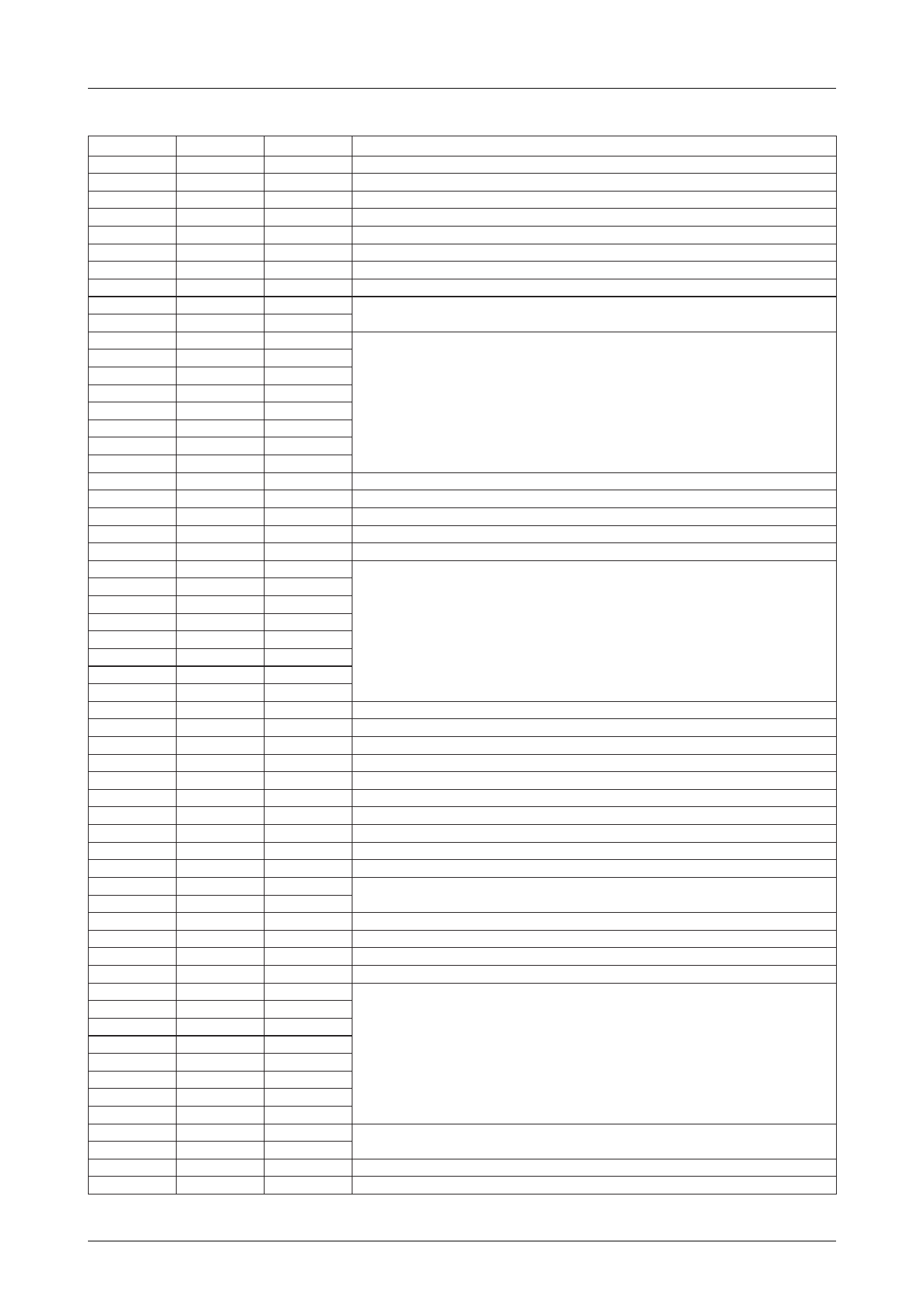
Pin Functions
Number
Name1
1
VSS
2
DATAEMP
3
UNDFLOW
4
BUFFULL
5
BUSY
6
XAPWR
7
XAPRD
8
XAPCS
9
SA0
10
SA1
11
SD0
12
SD1
13
SD2
14
SD3
15
SD4
16
SD5
17
SD6
18
SD7
19
XAPDTEN
20
VDD
21
VSS
22
XREAD
23
TEST
24
HD0
25
HD1
26
HD2
27
HD3
28
HD4
29
HD5
30
HD6
31
HD7
32
HDE
33
XSTEN
34
XDTEN
35
DRQWAIT
36
XCMD
37
XHRD
38
XHWR
39
CDPORT0
40
VDD
41
VSS
42
CDPORT1
43
CDPORT2
44
XAPTFR
45
XIORD
46
XIOWR
47
XCUSRIO
48
XCIO0
49
XCIO1
50
XCIO2
51
XCIO3
52
XCIO4
53
XCIO5
54
XCIO6
55
XCIO7
56
XCEXT0
57
XCEXT1
58
XCNVRAM
59
XCVSC
LC8953
I/O
Function
–
Ground pin
I
Data empty signal input pin for the LC8955
I
Underflow signal input pin for the LC8955
I
Buffer full signal input pin for the LC8955
I
Busy signal input pin for the LC8955
I
Data write signal input pin for the LC8955
I
Data read signal input pin for the LC8955
I
Chip select input pin for the LC8955
O
Resister select signal output pins for the LC8955
O
I/O
I/O
I/O
I/O
Data signal I/O pins for the LC8955
I/O
I/O
I/O
I/O
O
Data enable signal output pin for the LC8955 for automatic request transfer
–
+5V supply pin
–
Ground pin
I
Read signal input pin for the LC8955 for automatic request transfer
I
Test input pin (Tied low)
I/O
I/O
I/O
I/O
Data signal I/O pins for the LC8951 (RCHIP)
I/O
I/O
I/O
I/O
I
Erasure flag signal input pin for the LC8951 (RCHIP)
I
Status enable signal input pin for the LC8951 (RCHIP)
I
Data enable signal input pin for the LC8951 (RCHIP)
I
Data request/Wait select signal input pin for the LC8951 (RCHIP)
O
Command/Data select signal output pin for the LC8951 (RCHIP)
O
Data read signal output pin for the LC8951 (RCHIP)
O
Data write signal output pin for the LC8951 (RCHIP)
I/O
General-purpose input/output signal pin
–
+5V supply pin
–
Ground pin
I/O
General-purpose input/output signal pins
I/O
I
Mask operation select signal input pin for the LC8955 automatic request transfer
O
IC read signal output pin for Intel peripheral ICs
O
Write signal output pin for Intel peripheral ICs
O
User I/O address select signal output pin
O
O
O
O
Programmable I/O address select signal output pins
O
O
O
O
O
External address select signal output pins
O
O
NVRAM address select signal output pin
O
VSC address select signal output pin
Continued on next page.
No.3411–4/9
Share Link: 