CA3189 Просмотр технического описания (PDF) - Intersil
Номер в каталоге
Компоненты Описание
производитель
CA3189 Datasheet PDF : 8 Pages
| |||
CA3189
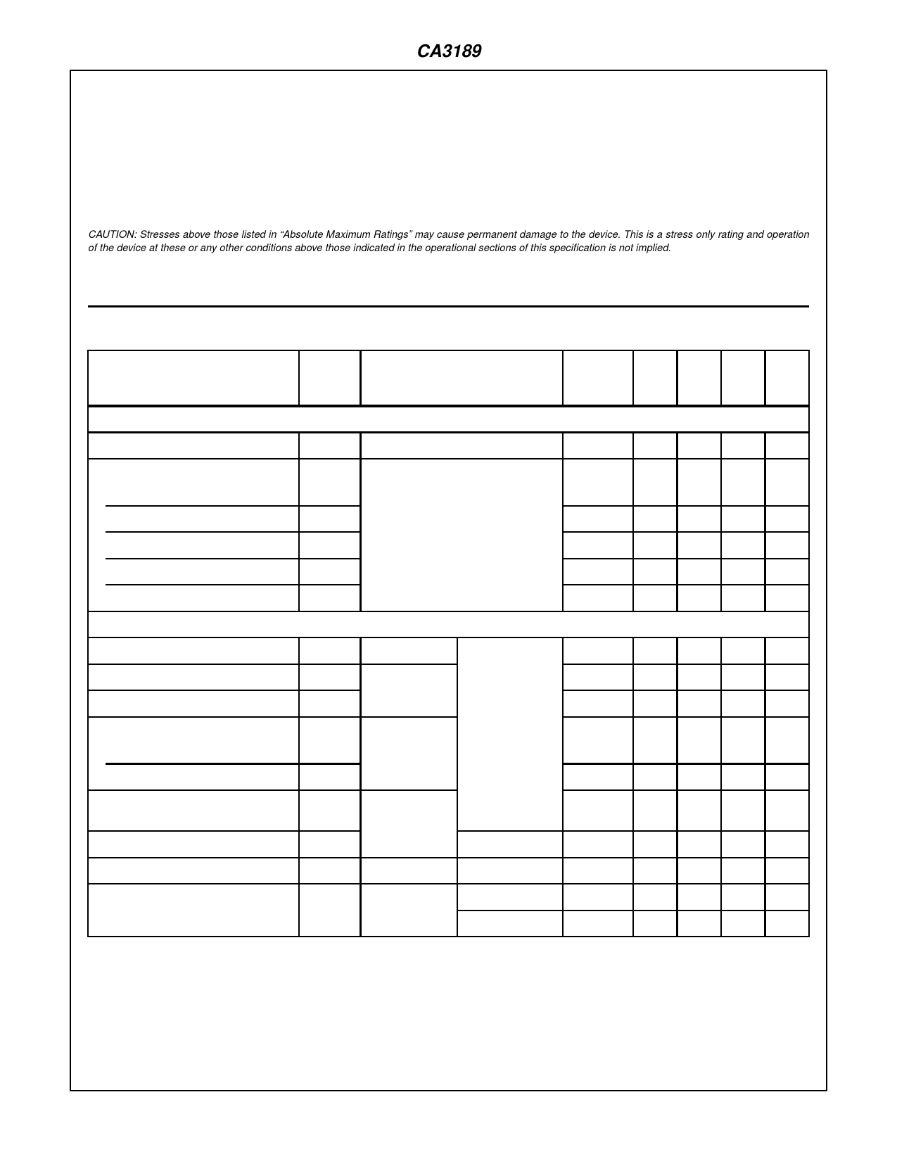
Absolute Maximum Ratings
DC Supply Voltage
(Between Terminals 11 and 4) . . . . . . . . . . . . . . . . . . . . . . . . 16V
(Between Terminals 11 and 14) . . . . . . . . . . . . . . . . . . . . . . . 16V
DC Current (Out of Terminal 15) . . . . . . . . . . . . . . . . . . . . . . . . 2mA
Operating Conditions
Temperature Range . . . . . . . . . . . . . . . . . . . . . . . . . -40oC to 85oC
Thermal Information
Thermal Resistance (Typical, Note 1)
θJA (oC/W)
PDIP Package . . . . . . . . . . . . . . . . . . . . . . . . . . . . .
90
Maximum Junction Temperature (Plastic Package) . . . . . . . . 150oC
Maximum Storage Temperature Range . . . . . . . . . -65oC to 150oC
Maximum Lead Temperature (Soldering 10s) . . . . . . . . . . . . 300oC
CAUTION: Stresses above those listed in “Absolute Maximum Ratings” may cause permanent damage to the device. This is a stress only rating and operation
of the device at these or any other conditions above those indicated in the operational sections of this specification is not implied.
NOTE:
1. θJA is measured with the component mounted on an evaluation PC board in free air.
Electrical Specifications TA = 25oC, V+ = 12V
PARAMETER
SYMBOL
TEST CONDITIONS
CIRCUIT
OR FIG.
NO.
MIN TYP MAX UNITS
DC SPECIFICATIONS
Quiescent Circuit Current
DC Voltages
Terminal 1 (IF Input)
Terminal 2 (AC Return to Input)
Terminal 3 (DC Bias to Input)
Terminal 15 (RF AGC)
Terminal 10 (DC Reference)
DYNAMIC SPECIFICATIONS
I11 No Signal Input, Non Muted
No Signal Input, Non Muted
V1
V2
V3
V15
V10
1, 2
20
31
40
mA
1, 2
1.2 1.9 2.4
V
1, 2
1.2 1.9 2.4
V
1, 2
1.2 1.9 2.4
V
1, 2
7.5 9.5 11
V
1, 2
5
5.6
6
V
Input Limiting Voltage (-3dB Point)
VI(lim)
fO = 10.7MHz,
1, 2
AM Rejection (Terminal 6)
AMR VIN = 0.1V,
fMOD. = 400Hz,
Deviation ±75kHz
1, 2
AM Mod. = 30%
Recovered AF Voltage (Terminal 6)
VO(AF)
1, 2
Total Harmonic Distortion (Note 2)
Single Tuned (Terminal 6)
THD VIN = 0.1V
1
Double Tuned (Terminal 6)
THD
2
-
12
25
µV
45
55
-
dB
325 500 650 mV
-
0.5
1
%
-
0.1
-
%
Signal Plus Noise to Noise Ratio
(Terminal 6)
S + N/N VIN = 0.1V
1, 2
65
72
-
dB
Deviation Mute Frequency
fDEV
fMOD = 0
1, 5, 6
-
±40
-
kHz
RF AGC Threshold
V16
1, 2
-
1.25
-
V
On Channel Step
V12 VIN = 0.1V
fDEV < ±40kHz
1
-
0
-
V
fDEV > ±40kHz
1
-
5.6
-
V
NOTE:
2. THD characteristics are essentially a function of the phase characteristics of the network connected between Terminals 8, 9, and 10.
2
Share Link: 