F25L016A Просмотр технического описания (PDF) - [Elite Semiconductor Memory Technology Inc.
Номер в каталоге
Компоненты Описание
производитель
F25L016A Datasheet PDF : 32 Pages
| |||
ESMT
F25L016A
Instructions
Instructions are used to Read, Write (Erase and Program), and
configure the F25L016A. The instruction bus cycles are 8 bits
each for commands (Op Code), data, and addresses. Prior to
executing any Byte-Program, Sector-Erase, Block-Erase, or
Chip-Erase instructions, the Write-Enable (WREN) instruction
must be executed first. The complete list of the instructions is
provided in Table 5. All instructions are synchronized off a high to
low transition of CE . Inputs will be accepted on the rising edge
of SCK starting with the most significant bit. CE must be driven
low before an instruction is entered and must be driven high after
the last bit of the instruction has been shifted in (except for Read,
Read-ID and Read-Status-Register instructions). Any low to high
transition on CE , before receiving the last bit of an instruction
bus cycle, will terminate the instruction in progress and return the
device to the standby mode.
Instruction commands (Op Code), addresses, and data are all
input from the most significant bit (MSB) first.
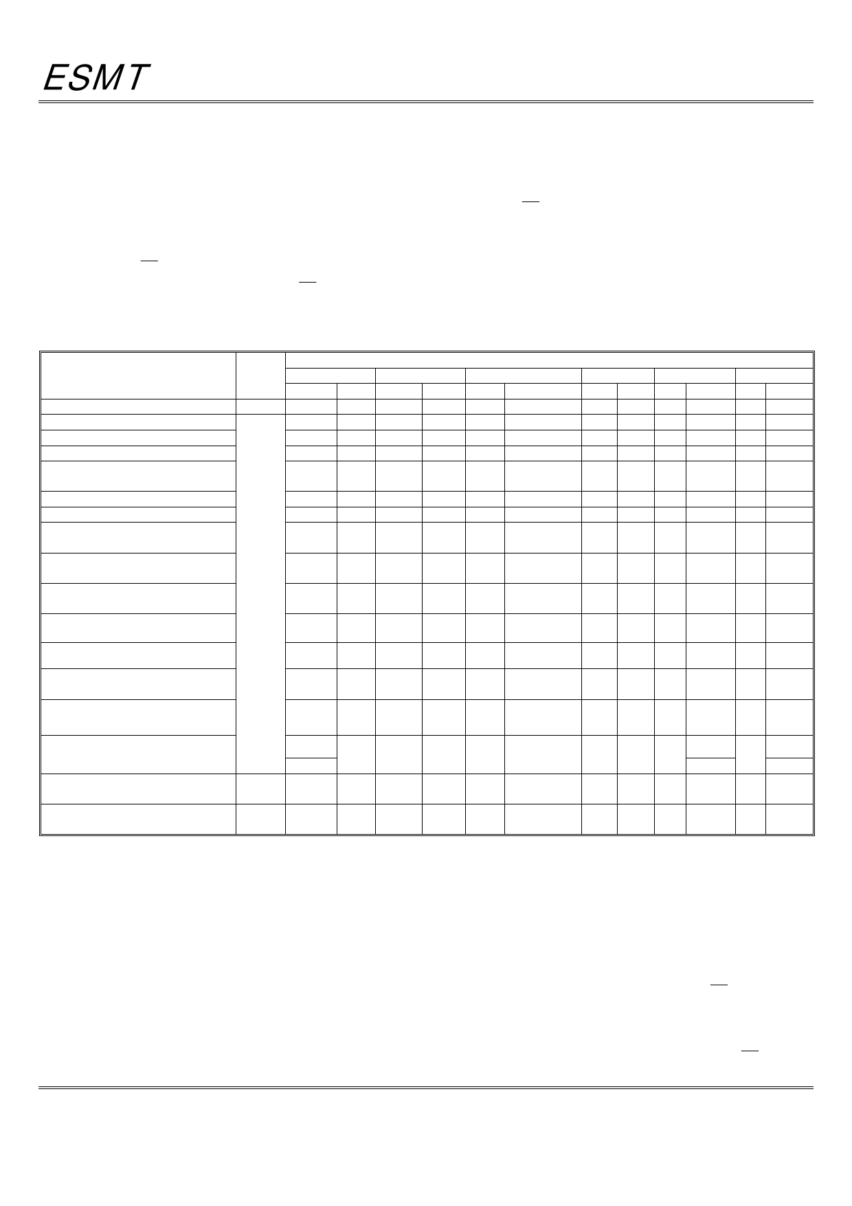
TABLE 5: DEVICE OPERATION INSTRUCTIONS
Cycle Type/
Operation1,2
Max
Freq
Read
High-Speed-Read
Sector-Erase4,5 (4K Byte)
Block-Erase (64K Byte)
33 MHz
Chip-Erase6
Byte-Program5
(AAI) Single-WORD Program5,6
Read-Status-Register
(RDSR)
50MHz
Enable-Write-Status-Register
(EWSR)8
Write-Status-Register
(WRSR)8
Write-Enable (WREN) 11
Write-Disable (WRDI)
100MHz
1
SIN
03H
0BH
20H
D8H
60H
C7H
02H
ADH
SOUT
Hi-Z
Hi-Z
Hi-Z
Hi-Z
Hi-Z
Hi-Z
Hi-Z
2
SIN SOUT
A23-A16 Hi-Z
A23-A16 Hi-Z
A23-A16 Hi-Z
A23-A16 Hi-Z
-
-
A23-A16 Hi-Z
A23-A16 Hi-Z
SIN
A15-A8
A15-A8
A15-A8
A15-A8
-
A15-A8
A15-A8
05H Hi-Z X DOUT -
50H Hi-Z -
-
-
01H Hi-Z Data Hi-Z -
06H Hi-Z -
04H Hi-Z -
-
-
-
-
Read-Electronic-Signature
(RES)
ABH Hi-Z X 14H -
Jedec-Read-ID (JEDEC-ID) 10
9FH Hi-Z X 8CH X
Bus Cycle
3
4
5
SOUT
SIN SOUT SIN SOUT
Hi-Z A7-A0 Hi-Z X DOUT
Hi-Z A7-A0 Hi-Z X
X
Hi-Z A7-A0 Hi-Z -
-
Hi-Z A7-A0 Hi-Z -
-
6
SIN SOUT
X DOUT
-
-
-
-
-
- --
-
-
-
Hi-Z
Hi-Z
Note7
A7-A0 Hi-Z DIN
A7-A0 Hi-Z DIN0
- Note7 -
Hi-Z -
Hi-Z DIN1
Note7 -
-
Hi-Z
-
-
- --
-
-
-
-
-. - -
-
-
-
-
- --
-
-
-
-
- --
-
-
-
-
- --
-
-
-
20H
X 15H -
-
-
-
Read-ID (RDID)
Enable SO to output RY/BY#
Status during AAI (EBSY)
Disable SO to output RY/BY#
Status during AAI (DBSY)
90H (A0=0) Hi-Z A23-A16 Hi-Z A15-A8
90H (A0=1)
-
70H Hi-Z -
-
-
-
80H Hi-Z -
-
-
Hi-Z
-
-
A7-A0 Hi-Z X
- --
- --
8CH
14H
-
-
X 14H
8CH
-
-
-
-
1. Operation: SIN = Serial In, SOUT = Serial Out
2. X = Dummy Input Cycles (VIL or VIH); - = Non-Applicable Cycles (Cycles are not necessary)
3. One bus cycle is eight clock periods.
4. Sector addresses: use AMS-A12, remaining addresses can be VIL or VIH
5. Prior to any Byte-Program, Sector-Erase , Block-Erase ,or Chip-Erase operation, the Write-Enable (WREN) instruction must be
executed.
6. To continue programming to the next sequential address location, enter the 8-bit command, ADH, followed by the data to be
programmed.
7. The Read-Status-Register is continuous with ongoing clock cycles until terminated by a low to high transition on CE .
8. The Enable-Write-Status-Register (EWSR) instruction and the Write-Status-Register (WRSR) instruction must work in conjunction
of each other. The WRSR instruction must be executed immediately (very next bus cycle) after the EWSR instruction to make both
instructions effective.
9. The Read-Electronic-Signature is continuous with on going clock cycles until terminated by a low to high transition on CE .
10. The Jedec-Read-ID is output first byte 8CH as manufacture ID; second byte 20H as top memory type; third byte 15H as memory
Elite Semiconductor Memory Technology Inc.
Publication Date: Jul. 2008
Revision: 1.4
10/32
Share Link: 