DRF100 Просмотр технического описания (PDF) - Advanced Power Technology
Номер в каталоге
Компоненты Описание
производитель
DRF100 Datasheet PDF : 12 Pages
| |||
Driver Specifications
Symbol Parameter
tr
Rise Time 2,3
tf
Fall Time 2,3
TD
Prop. Delay 2,4
Symmetry 1
TJ = 25°C unless otherwise specified
Test Conditions
Min
15VDD
15VDD
15V
15VDD 3
Typical
RL
CL
3.1 7.5
2.8 7.5
33 38
1.2
DRF100
Max Unit
ns
%
Driver Output Characteristics
Symbol Parameter
Cout
Rout
Lout
FMAX
Output Capacitance 2,5
Output Resistance 2,5
Output Inductance 2,5
Operating Frequency
TJ = 25°C unless otherwise specified
Min Typ
2500
1
2
3
Test curcuit show on page 3.
All measurements were made with the Anti-Ring circuit activated unless noted.
1. Symmetry is the percent difference in high and low FWHM times with a 50% duty cycle square wave input.
2 RL = 50Ω, CL = 3000pF
3 10% - 90% See Test Circuit
4 50% - 50%, see Test Circuit
5 VDD = 18V, CL = 3000pF, F = 10MHz
6 Performance specified with this input.
APT reserves the right to change, without notice, the specifications and information contained herein.
Max
4
30
Unit
pF
Ω
nH
MHz
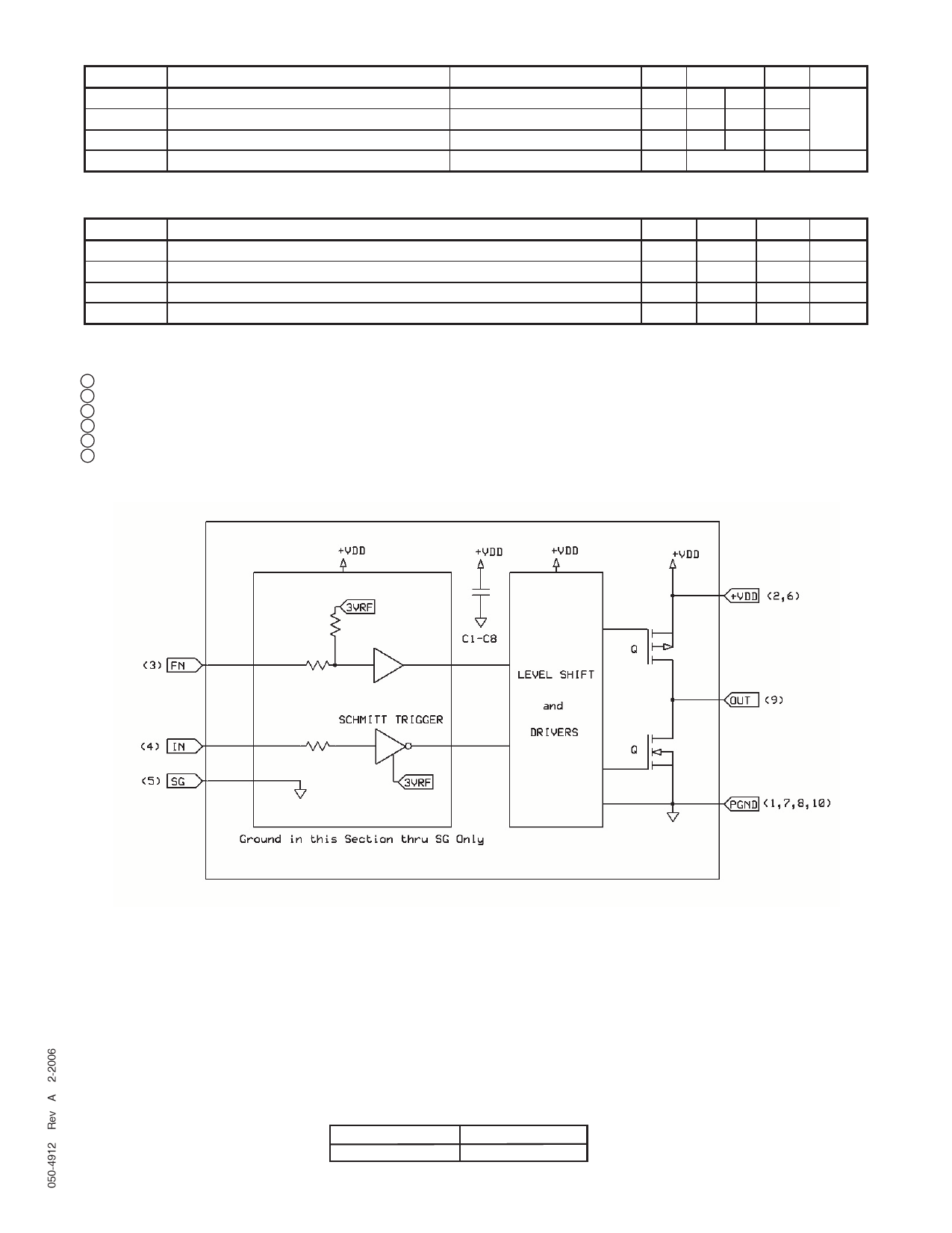
Figure 1, DRF100 Simplified Ciruit Diagram
A Simplified DRF100 Circuit Diagram is illustrated above. By including the driver high speed by-pass capacitors (C1-
C8), their contribution to the internal parasitic loop inductance of the driver output is greatly reduced. This, coupled with
the tight geometry of the hybrid, allows optimum drive to the gate of the MOSFET. This low parasitic approach, coupled
with the Schmitt trigger input, Kelvin signal ground (4,5) and the Anti-Ring Function, provide improved stability and
control in Kilowatt to Multi-Kilowatt, High Frequency applications
The IN pin (4) is applied to a Schmitt Trigger. The signal is then applied to the intermediate drivers and level shifters;
this section contains proprietary circuitry designed specifically for ring abatement. The P channel and N channel power
drivers provide the high current to the OUT pin (9).
The FUNCTION, FN, pin (3) is used to disable the Anti-Ring function. It is recommended that the device be operated
with this function enabled. Func. = Hi (+5V or Float) Anti-Ring on, Func. = Low (0V or GND.) Anti-ring off.
Driver Control Logic
In (4) HIGHDriver Output (9) LOW
In (4) LOWDriver Output (9) HIGH
Share Link: 