HDMP-1512 Просмотр технического описания (PDF) - HP => Agilent Technologies
Номер в каталоге
Компоненты Описание
производитель
HDMP-1512 Datasheet PDF : 26 Pages
| |||
INTERNAL INPUT
DATA SELECT
STREAM
± SI
11
12
VCC_LZ1 16
VCC_LZ
23
24
GND_LZ
25
26
MUX
-LZON 30
LZPWRON 36
LASER ON
FAULT 29
ERROR
DETECTOR
AC AMP
DISABLE
WINDOW
DETECTOR
Tx CHIP BOUNDARY
+
AC AMP
–
VCC_LZAC 5 Ω
17
VCC
0.1 µF
0.1 µF
+LZOUT
19
-LZOUT
20
25 Ω TRANSMISSION LINE
LZCSE
14
POT 2
50 Ω
5Ω
0.1 µF
25 Ω
LZDC
–
DC
OP-AMP
0.1 µF
21
+
10 nF
10 nF
0.1 µF
VCC
P2
301 Ω
EXTERNAL
CONTROL
2.2 Ω
BANDGAP
REFERENCE
P1 (β >= 100)
8Ω
0.1 µF
25 Ω
BANDGAP
DETECTOR
15
VCC-LZBG
27
LZTC
0.1 µF
28 22
LZBTP
LZMDF
POT 1 5 KΩ
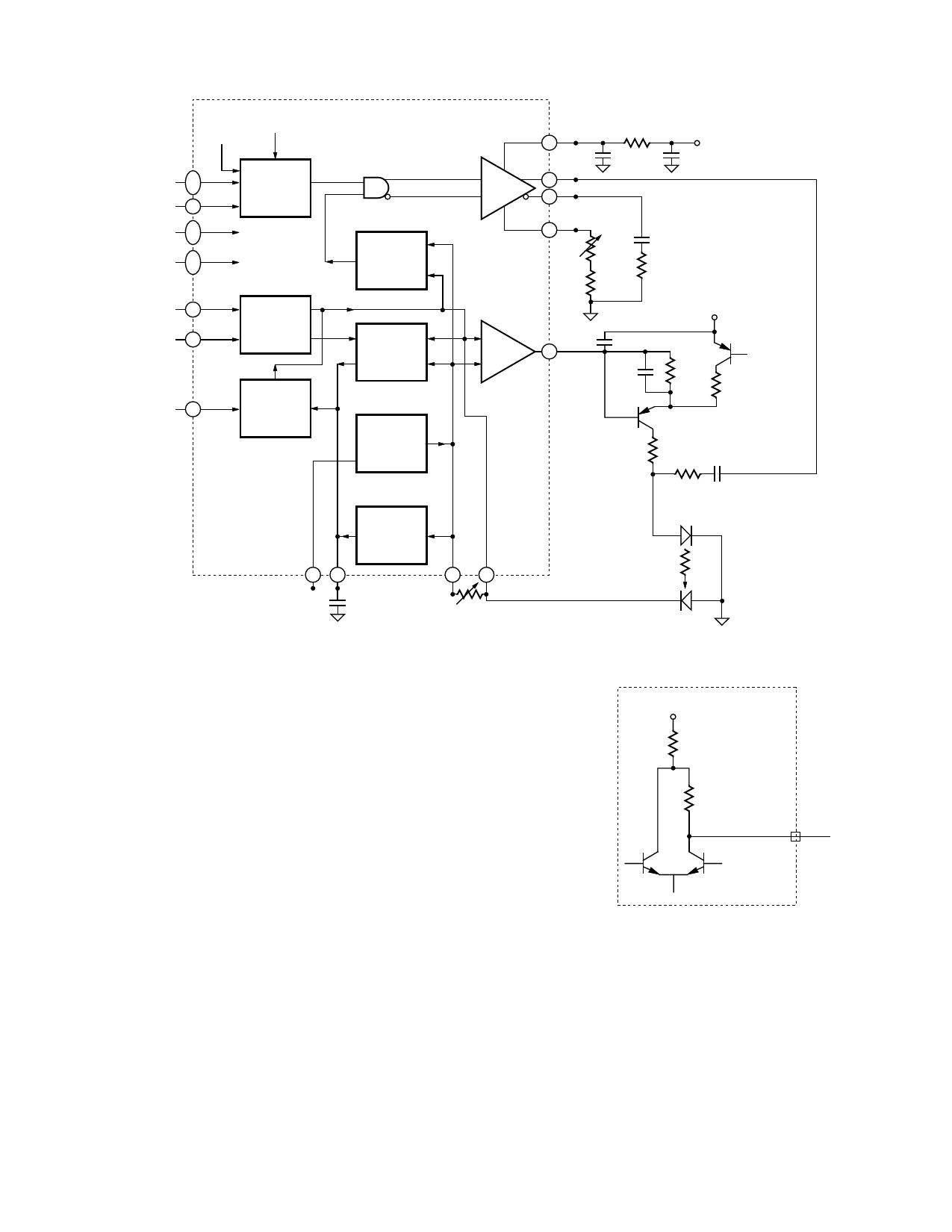
Figure 3. Laser Driver Block Diagram and External Circuitry.
described in more detail in the
laser driver operation section
below.
Transmitter Laser Driver
Operation
The block diagram of the HDMP-
1512, Tx, laser driver circuitry is
shown in Figure 3. The laser
driver is enabled by setting
-LZON (pin 30) low and
LZPWRON (pin 36) high. The
circuitry in Figure 3, shown
outside the chip boundary (dotted
box), illustrates the external
components required to complete
a typical laser driver connection.
The input data source to the laser
driver is user selected from either
the internally generated data
stream, or an externally supplied
high speed data stream. The
externally supplied data stream is
applied to the high speed input
± SI pins. The user selects
between these two data sources
through the proper settings of
pins TS1, TS2, and EWRAP (pins
76, 75, and 71). The possible
combinations of active inputs and
outputs are shown in the Input/
Output Select Table. The chosen
high speed input is then modu-
lated onto the laser by the ac
amplifier. The external poten-
tiometer, Pot 2, shown connected
to pin LZCSE (# 14) is used to
adjust the laser modulation
depth. The laser driver output is
at pins 19 and 20, ± LZOUT.
Laser diode dc bias control is
provided through the LZDC
(# 21) pin. Adjustment of Pot 1
sets the nominal dc bias desired
for the laser diode. The
equivalent output circuit of LZDC
is shown in Figure 4. Laser diode
fault and safety control is imple-
mented through the combination
VCC_LZ
54
400
LZDC
Figure 4. LZDC Equivalent Output
Circuit (Tx pin # 21).
of the window detector, error
detector, Laser On pin # 30
(-LZON), laser monitor diode
feedback pin # 22 (LZMDF), and
the op-amp dc bias control
circuit. The window detector
monitors the voltage on pin
LZMDF. If this voltage goes out
of range by more than ± 10%
from the nominal setting, the
659
Share Link: 