CXB1581Q Просмотр технического описания (PDF) - Sony Semiconductor
Номер в каталоге
Компоненты Описание
производитель
CXB1581Q Datasheet PDF : 22 Pages
| |||
CXB1581Q
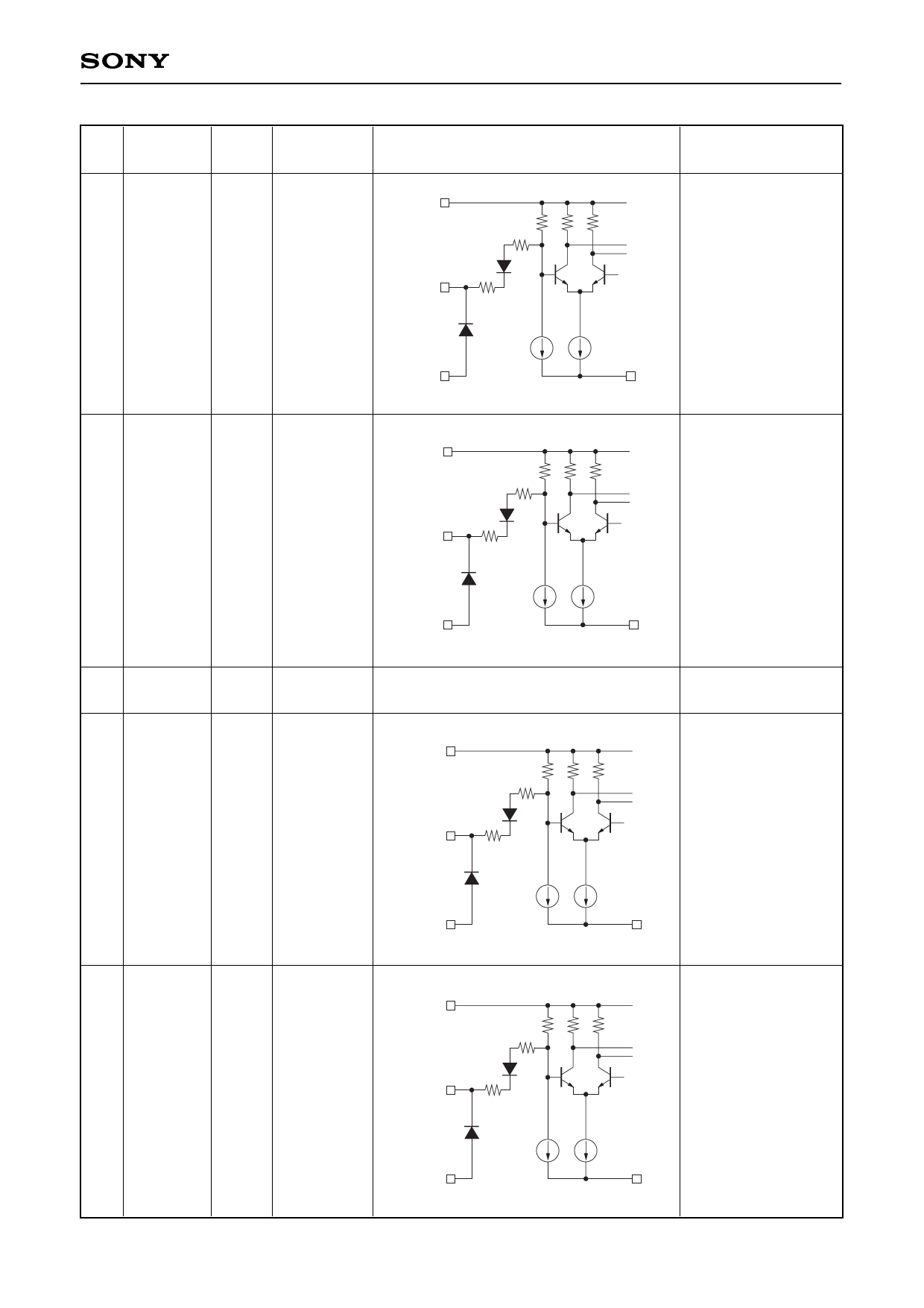
Pin
No.
Symbol
Type
Typical pin
I/O voltage
Equivalent circuit
VCCG
38 TPGEN
TTL
input
TTL level
TPGEN
VEET
Description
Test pattern
generation control.
Inputting high level
to this pin generates
positive or alternating
disparity K28.5 (one
of the 8B10B
conversion codes) as
the serial transfer
VEET data.
VCCG
39 ALTSEL∗
TTL
input
TTL level
ALTSEL∗
40,
41
NC
Open
VEET
VCCG
42
ECLKSEL∗
TTL
input
TTL high
level or 3.3V
ECLKSEL∗
VEET
Alternating disparity
selection. The test
pattern generated
when TPGEN is set
to high level
becomes alternating
disparity K28.5 if this
pin is set to low level,
and positive disparity
K28.5 if this pin is set
VEET to high level.
No connection.
External clock
selection. When this
pin is set to low level,
the clock input to
EXCLK is used as
the transmission bit
clock.
VEET
VCCG
43
TCLKSEL∗
TTL
input
TTL high
level or 3.3V
TCLKSEL∗
VEET
–7–
Transmission bit
clock output
selection. When this
pin is set to low level,
the transmission bit
clock is output from
PSOUT. (See Table
1.)
VEET
Share Link: 