CXB1581Q Просмотр технического описания (PDF) - Sony Semiconductor
Номер в каталоге
Компоненты Описание
производитель
CXB1581Q Datasheet PDF : 22 Pages
| |||
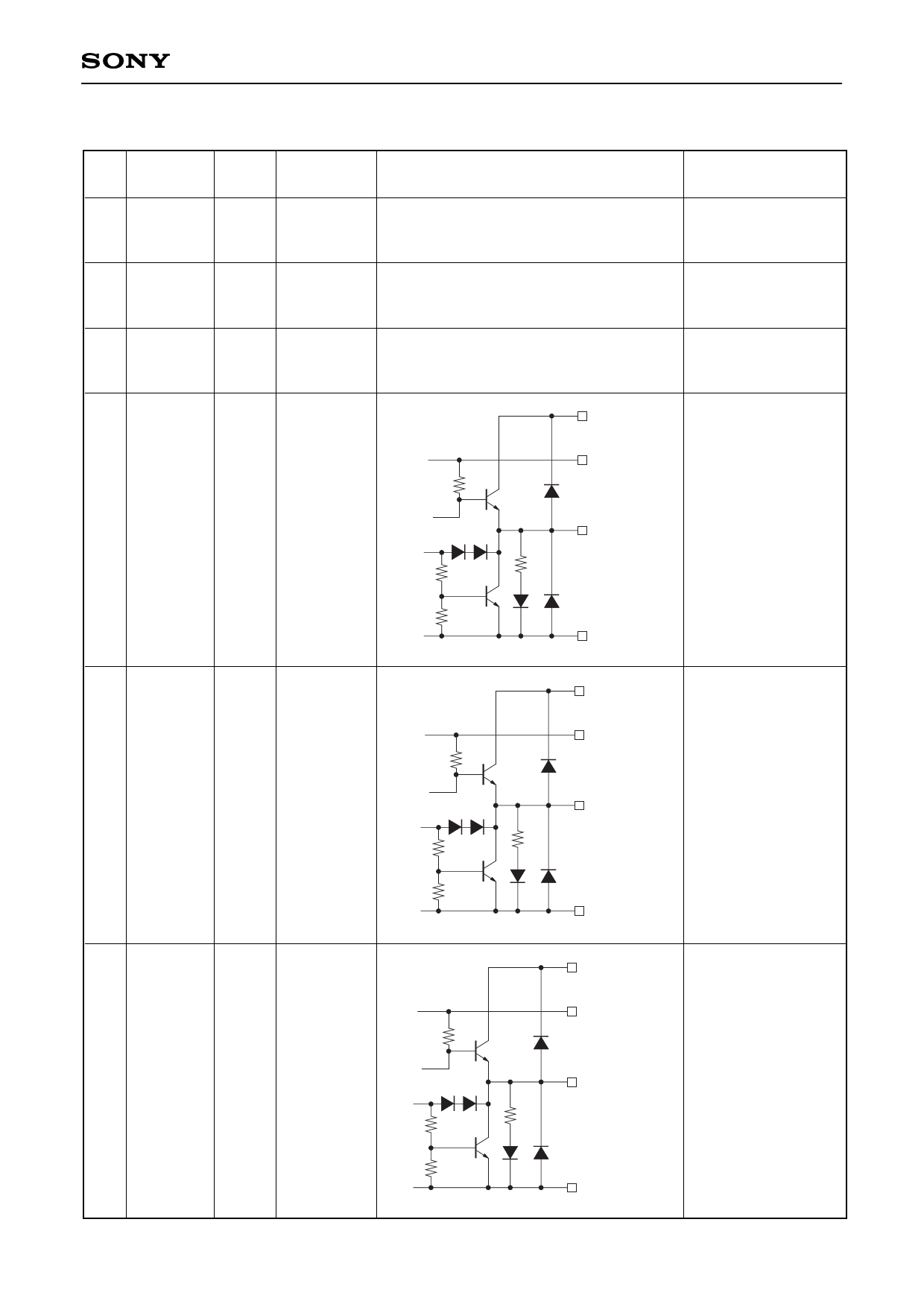
Pin Description
Pin
No.
Symbol
Type
Typical pin
I/O voltage
1, 21,
32, 49
VEEG
Power
supply
0V
2, 20,
33,50, VCCG
51
Power
supply
3.3V
3, 4 VEET
Power
supply
0V
5 LKDT∗
TTL
output
TTL level
6 FAULT
TTL
output
TTL level
7
TBC_OUT
TTL
output
TTL level
CXB1581Q
Equivalent circuit
—
—
—
VCCT5
VCCT3
LKDT∗
VEET
VCCT5
VCCT3
FAULT
VEET
VCCT5
VCCT3
TBC_OUT
–4–
VEET
Description
Negative power
supplies for internal
logic gate.
Positive power
supplies for internal
logic gate.
Negative power
supplies for TTL
output.
PLL lock detection
signal output. This
pin outputs low level
when the PLL is
locked to TBC_IN
and operating
normally, and high
level when the PLL
is not operating
normally.
FAULT signal output.
This pin is used for
the FAULT signal in
the GLM standard.
This pin outputs high
level at the rising
edge of LDALM and
low level at the falling
edge of R_RLT. (See
Table 3.)
Transmission byte
clock output
(53.125MHz).
This clock is
generated by
frequency-dividing
the transmission bit
clock (1.0625GHz or
531.25MHz).
Share Link: 