TQ9303 Просмотр технического описания (PDF) - TriQuint Semiconductor
Номер в каталоге
Компоненты Описание
производитель
TQ9303 Datasheet PDF : 25 Pages
| |||
TQ9303
Line State Decoder Block
Parity Generator Block
The state machine that indicates line state status
simply looks for three consecutive line state primitives
(that is, three of a kind in a row) to achieve a particular
Fibre Channel line state. Line states are used in link
initialization protocol, as described in the Fibre Channel
specification (FC-PH). A subset of the ordered sets, line
states are Fibre Channel primitive sequences which
provide information regarding the condition of the link.
The following are the four line states:
• Off-Line State (OLS) indicates either an internal
port failure or a transmitter power down/
diagnostics performance / initialization.
• Non-Operational State (NOS) signals a link failure.
• Link Reset (LR) recognizes the OLS and port reset
conditions.
• Link Reset Response (LRR) recognizes a link reset.
These line states are defined in Appendix␣ B. The Line
State Decoder generates CRXS2..3, the line state status
bits which advise the host as to the state of the Sync
State Machine, and CRXS4..5, the line state ID bits
which signal the occurrance of certain primitive
sequences. The status bits are shown in Tables 2 and 3.
Four parity bits (CTXP0..3) are generated by the Parity
Generator. Each parity bit corresponds to a byte of
data, as follows: CRXP0 to CRXD0..7, CRXP1 to
CRXD8..15, CRXP2 to CRXD16..23, and CRXP3 to
CRXD24..31.
Control bit RXPMODE (Receive Parity MODE) alters the
normal meaning of CRXP3. RXPMODE low is the
normal mode, where CRXP3 generates parity for
CRXD24..31. With RXPMODE high, however, CRXP3
generates parity for CRXD24..31 and CRXS0. CRXS0 is
a control output that indicates whether CTXD0..31 is
data or an ordered set.
The parity bits follow odd parity convention, where it is
high if the number of ones is even and low if the
number of ones is odd.
In Raw mode, the Parity Generator does not generate
parity, and the output parity bits are mapped with the
input data as shown in Table␣ 1.
Clock Generator Block
32-Bit CRC Checker Block
The CRC Checker computes the 32-bit cyclic
redundancy check on the received data. The CRC Error
Status bit CRXS1 is driven high when an error is
detected. In Raw mode, CRC is not checked, and
CRXS1 is driven low.
The Clock Generator generates word, half-word, and
byte clocks required by other blocks in the Decoder.
The Clock Generator uses the recovered clock, BRXCLK,
generated by the TQ9502 Receiver. For example, using
Fibre Channel data rates, BRXCLK (a byte clock) runs at
106.25␣ MHz using FC1063, 53.125␣ MHz using FC531,
and 26.5625␣ MHz using FC266.
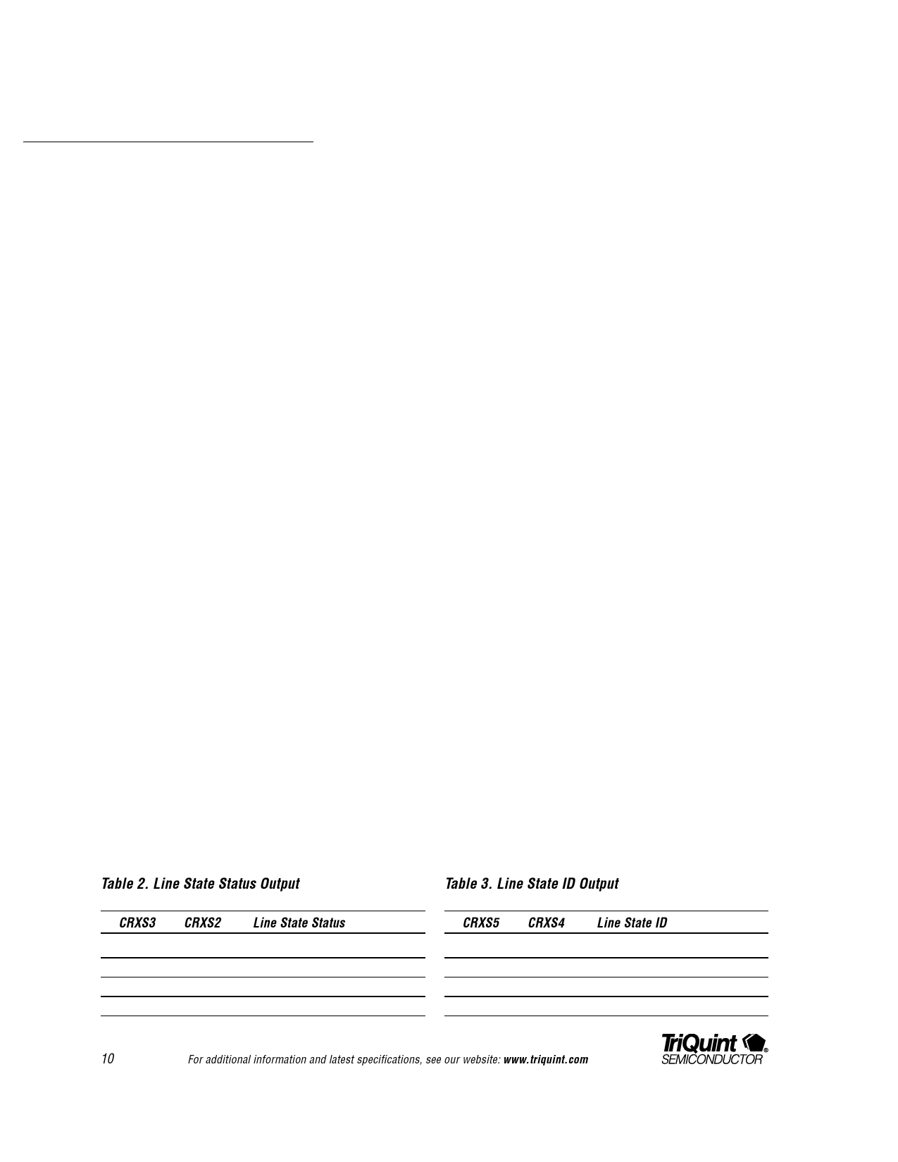
Table 2. Line State Status Output
CRXS3
0
0
1
1
CRXS2
0
1
0
1
Line State Status
No State
Pending State
In State
Invalid Sequence
Table 3. Line State ID Output
CRXS5
0
0
1
1
CRXS4
0
1
0
1
Line State ID
NOS – Non-Operational State
OLS – Off-Line State
LR – Link Reset
LRR – Link Reset Response
10
For additional information and latest specifications, see our website: www.triquint.com
Share Link: 