CMM2030-BD Просмотр технического описания (PDF) - Mimix Broadband
Номер в каталоге
Компоненты Описание
производитель
CMM2030-BD Datasheet PDF : 8 Pages
| |||
30.0 kHz-30.0 GHz GaAs MMIC
Distributed Amplifier
May 2010 - Rev 07-May-10
CMM2030-BD
App Note [1] Biasing - As shown in the bonding diagram, this device
is operated with a single drain and gate voltage via RF Out and RF In,
respectively. Bias is nominally Vd=5.0V and Id=100mA. It is
recommended to use active biasing to keep the currents constant as
the RF power and temperature vary; this gives the most reproducible
results. Depending on the supply voltage available and the power
dissipation constraints, the bias circuit may be a single transistor or a
low power operational amplifier, with a low value resistor in series with
the drain supply used to sense the current. The gate of the pHEMT is
controlled to maintain correct drain current and thus drain voltage. The typical gate voltage needed to do this is 0.5V. Typically
the gate is protected with Silicon diodes to limit the applied voltage. Also, make sure to sequence the applied voltage to
ensure negative gate bias is available before applying the positive drain supply.
App Note [2] Bias Arrangement - Each DC pad (EXT1,2) need to have DC bypass capacitance (117 pF, 560 pF, 0.33 uF)
as close to the device as possible.
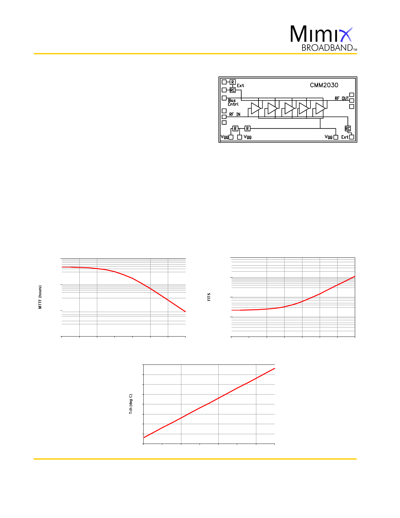
MTTF Graphs
These numbers were calculated based upon accelerated life test information received from the fabricating foundry and extensive thermal modeling/
finite element analysis done at Mimix Broadband. The values shown here are only to be used as a guideline against the end application requirements
and only represent reliability information under one bias condition. Ultimately bias conditions and resulting power dissipation along with the
practical aspects, i.e. thermal material stack-up, attach method of device placement are the key parts in determining overall reliability for a specific
application, see previous pages. If the data shown below does not meet your reliability requirements or if the bias conditions are not within your
operating limits please contact technical sales for additional information.
1.0E+09
CMM2030-BD Vd=5.0 V, Id=100 mA
1.00E+00
CMM2030-BD Vd=5.0 V, Id=100 mA
1.0E+08
1.0E+07
1.00E-01
1.00E-02
1.00E-03
1.0E+06
55
65
75
85
95
105
115
125
Backplate Temperature (deg C)
1.00E-04
55
65
75
85
95
105
115
125
Baseplate Temperature (deg C)
CMM2030-BD Vd=5.0 V, Id=100 mA
140
130
120
110
100
90
80
70
60
55
65
75
85
95
105
115
125
Backplate Temperature (deg C)
Mimix Broadband, Inc., 10795 Rockley Rd., Houston, Texas 77099
Tel: 281.988.4600 Fax: 281.988.4615 mimixbroadband.com
Page 7 of 8
Characteristic Data and Specifications are subject to change without notice. ©2010 Mimix Broadband, Inc.
Export of this item may require appropriate export licensing from the U.S. Government. In purchasing these parts, U.S. Domestic customers accept
their obligation to be compliant with U.S. Export Laws.
Share Link: 