CAV24C02(2015) Просмотр технического описания (PDF) - ON Semiconductor
Номер в каталоге
Компоненты Описание
производитель
CAV24C02 Datasheet PDF : 15 Pages
| |||
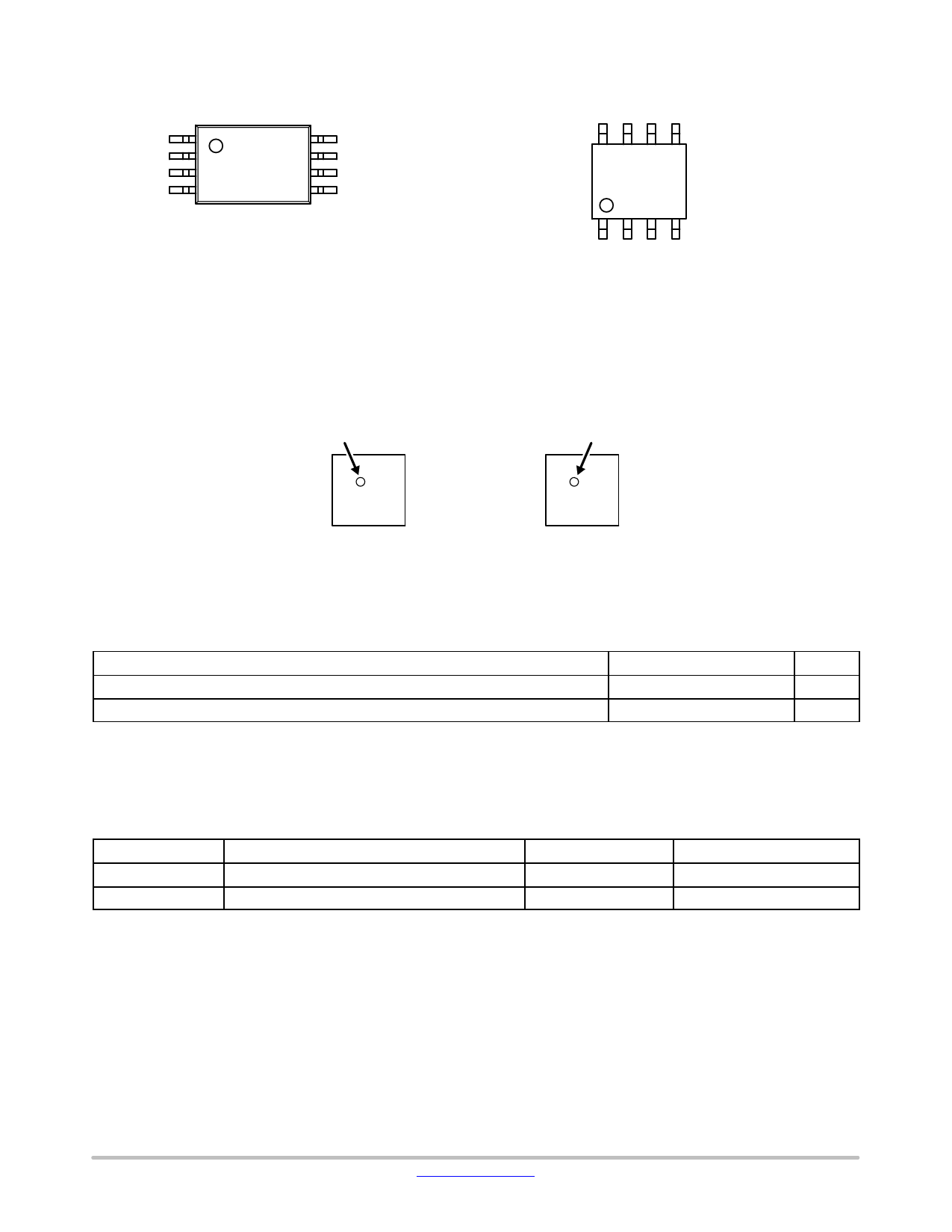
CAV24C02, CAV24C04, CAV24C08, CAV24C16
(TSSOP−8)
DEVICE MARKINGS
(SOIC−8)
CSSS
AYMXXX
G
CSSS
SSS
SSS
SSS
SSS
A
Y
M
XXX
G
= Specific Device Code, where
= 02H for CAV24C02
= 04K for CAV24C04
= 08K for CAV24C08
= 16K for CAV24C16
= Assembly Location
= Production Year (Last Digit)
= Production Month (1−9, O, N, D)
= Last Three Digits of Assembly Lot Number
= Pb−Free Package
24CSSS
AYMXXX
G
24CSSS = Specific Device Code, where
SSS = 02H for CAV24C02
SSS = 04K for CAV24C04
SSS = 08K for CAV24C08
SSS = 16K for CAV24C16
A
= Assembly Location
Y
= Production Year (Last Digit)
M
= Production Month (1−9, O, N, D)
XXX = Last Three Digits of Assembly Lot Number
G
= Pb−Free Package
Pin 1 TOP MARKING FOR WLCSP Pin 1
(Ball Down)
X
YM
WLCSP−4
X = Specific Device
X = Code
4 = 24C04
8 = 24C08
6 = 24C16
X
YM
WLCSP−5
Y = Production Year (Last Digit)
M = Production Month (1−9, O, N, D)
Table 1. ABSOLUTE MAXIMUM RATINGS
Parameters
Ratings
Units
Storage Temperature
−65 to +150
°C
Voltage on any pin with respect to Ground (Note 1)
−0.5 to +6.5
V
Stresses exceeding those listed in the Maximum Ratings table may damage the device. If any of these limits are exceeded, device functionality
should not be assumed, damage may occur and reliability may be affected.
1. During input transitions, voltage undershoot on any pin should not exceed −1 V for more than 20 ns. Voltage overshoot on pins A0, A1, A2
and WP should not exceed VCC + 1 V for more than 20 ns, while voltage on the I2C bus pins, SCL and SDA, should not exceed the absolute
maximum ratings, irrespective of VCC.
Table 2. RELIABILITY CHARACTERISTICS (Note 2)
Symbol
Parameter
Min
Units
NEND (Note 3)
Endurance
1,000,000
Program / Erase Cycles
TDR
Data Retention
100
Years
2. These parameters are tested initially and after a design or process change that affects the parameter according to appropriate AEC−Q100
and JEDEC test methods.
3. Page Mode, VCC = 5 V, 25°C.
www.onsemi.com
2
Share Link: 