PI74FCT162646T Просмотр технического описания (PDF) - Pericom Semiconductor
Номер в каталоге
Компоненты Описание
производитель
PI74FCT162646T Datasheet PDF : 8 Pages
| |||
PI74FCT16646T/162646T/162H646T
11223344556677889900112233445566778899001122334455667788990011221122334455667788990011223344556677889900112233445566778899001122112233445566778899001122334455667788990011223344556677889900112211223314465566-77B8899i00t1122R3344e55g6677i88s99t00e11r2233e44d556677T8899r00a1122n11s2233c44e55i66v7788e99r00s1122
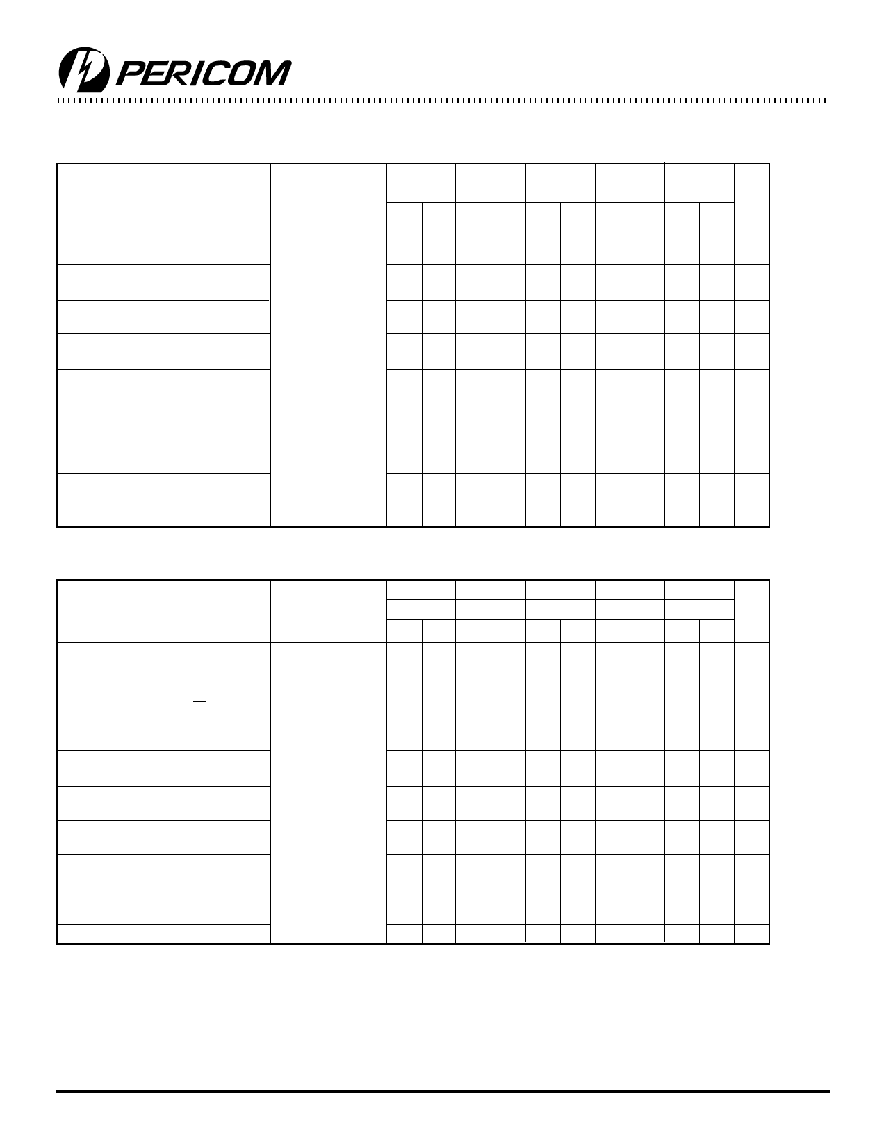
PI74FCT16646T Switching Characteristics over Operating Range
Parameters Description
Conditions(1)
16646T 16646AT 16646CT 16646DT 16646ET
Com.
Com.
Com.
Com.
Com.
Min. Max. Min. Max. Min. Max. Min. Max. Min. Max. Units
tPLH
tPHL
tPZH
tPZL
tPHZ
tPLZ
tPLH
tPHL
tPLH
tPHL
tSU
tH
tW
tSK(o)
Propagation Delay
Bus to Bus
Output Enable Time
xDIR or xOE to Bus
Output Disable Time(3)
xDIR or xOE to Bus
Propagation Delay
Clock to Bus
Propagation Delay
xSBA or xSAB to Bus
Setup Time HIGH or
LOW, BUS to Clock
Hold Time HIGH or
LOW, Bus to Clock
Clock Pulse Width
HIGH or LOW(3)
Output Skew(4)
CL = 50 pF
RL = 500Ω
2.0 9.0 2.0 6.3 1.5 5.4 1.5 4.4 1.5 3.8 ns
2.0 14.0 2.0 9.8 1.5 7.8 1.5 5.0 1.5 4.8 ns
2.0 9.0 2.0 6.3 1.5 6.3 1.5 4.3 1.5 4.0 ns
2.0 9.0 2.0 6.3 1.5 5.7 1.5 4.4 1.5 3.8 ns
2.0 11.0 2.0 7.7 1.5 6.2 1.5 5.0 1.5 4.2 ns
4.0 — 2.0 — 2.0 — 2.0 — 2.0 — ns
2.0 — 1.5 — 1.5 — 1.0 — 0.0 — ns
6.0 — 5.0 — 5.0 — 3.0 — 3.0 — ns
— 0.5 — 0.5 — 0.5 — 0.5 — 0.5 ns
PI74FCT162646T Switching Characteristics over Operating Range
Parameters Description
Conditions(1)
162646T 162646AT 162646CT 162646DT 162646ET
Com.
Com.
Com.
Com.
Com.
Min. Max. Min. Max. Min. Max. Min. Max. Min. Max. Units
tPLH
tPHL
tPZH
tPZL
tPHZ
tPLZ
tPLH
tPHL
tPLH
tPHL
tSU
tH
tW
tSK(o)
Propagation Delay
Bus to Bus
Output Enable Time
xDIR or xOE to Bus
Output Disable Time(3)
xDIR or xOE to Bus
Propagation Delay
Clock to Bus
Propagation Delay
xSBA or xSAB to Bus
Setup Time HIGH or
LOW, BUS to Clock
Hold Time HIGH or
LOW, Bus to Clock
Clock Pulse Width
HIGH or LOW(3)
Output Skew(4)
CL = 50 pF
RL = 500Ω
2.0 9.0 2.0 6.3 1.5 5.4 1.5 4.4 1.5 3.8 ns
2.0 14.0 2.0 9.8 1.5 7.8 1.5 5.0 1.5 4.8 ns
2.0 9.0 2.0 6.3 1.5 6.3 1.5 4.3 1.5 4.0 ns
2.0 9.0 2.0 6.3 1.5 5.7 1.5 4.4 1.5 3.8 ns
2.0 11.0 2.0 7.7 1.5 6.2 1.5 5.0 1.5 4.2 ns
4.0 — 2.0 — 2.0 — 2.0 — 2.0 — ns
2.0 — 1.5 — 1.5 — 1.0 — 0.0 — ns
6.0 — 5.0 — 5.0 — 3.0 — 3.0 — ns
— 0.5 — 0.5 — 0.5 — 0.5 — 0.5 ns
Notes:
1. See test circuit and wave forms.
2. Minimum limits are guaranteed but not tested on Propagation Delays.
3. This parameter is guaranteed but not production tested.
4. Skew between any two outputs, of the same package, switching in the same direction. This parameter is guaranteed by design.
7
PS2039B 02/24/99
Share Link: 