ATT3042 Просмотр технического описания (PDF) - Unspecified
Номер в каталоге
Компоненты Описание
производитель
ATT3042 Datasheet PDF : 80 Pages
| |||
ATT3000 Series Field-Programmable Gate Arrays
Data Sheet
February 1997
Programmable Interconnect (continued)
General-Purpose Interconnect
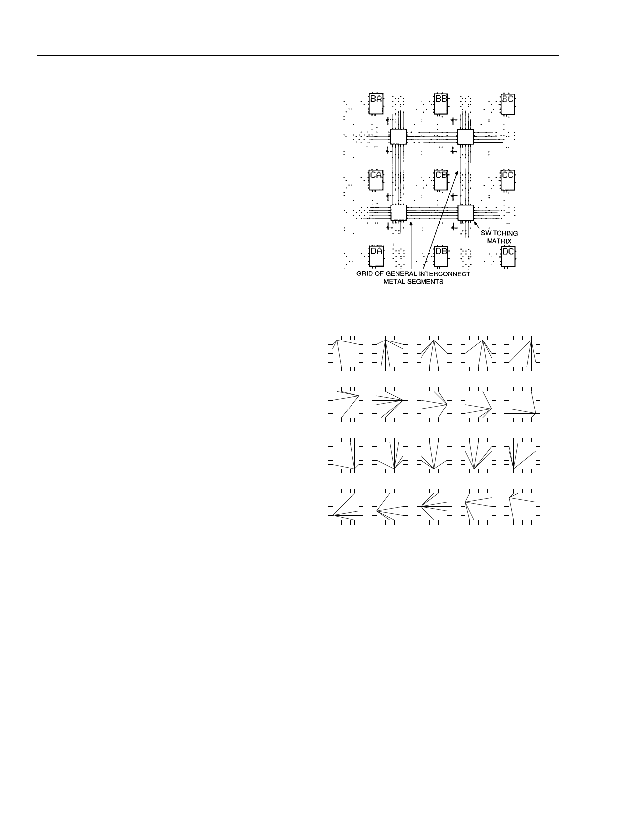
General-purpose interconnect, as shown in Figure 9,
consists of a grid of five horizontal and five vertical
metal segments located between the rows and col-
umns of logic and IOBs. Each segment is the height or
width of a logic block. Switching matrices join the ends
of these segments and allow programmed interconnec-
tions between the metal grid segments of adjoining
rows and columns. The switches of an unprogrammed
device are all nonconducting. The connections through
the switch matrix may be established by automatic or
interactive routing by selecting the desired pairs of
matrix pins to be connected or disconnected. The
legitimate switching matrix combinations for each pin
are indicated in Figure 10.
Special buffers within the general interconnect areas
provide periodic signal isolation and restoration for
improved performance of lengthy nets. The intercon-
nect buffers are available to propagate signals in either
direction on a given general interconnect segment.
These bidirectional (bidi) buffers are found adjacent to
the switching matrices, above and to the right. The
other PIPs adjacent to the matrices are accessed to or
from long lines. The development system automatically
defines the buffer direction based on the location of the
interconnection network source. The delay calculator in
the ORCA Foundry Development System automatically
calculates and displays the block, interconnect, and
buffer delays for any paths selected. Generation of the
simulation netlist with a worst-case delay model is also
provided by the development system.
Some of the interconnect PIPs are directional, as
indicated below:
s ND is a nondirectional interconnection.
s D:H->V is a PIP which drives from a horizontal to a
vertical line.
s D:V->H is a PIP which drives from a vertical to a
horizontal line.
s D:C->T is a T-PIP which drives from a cross of a
T to the tail.
s D:CW is a corner PIP which drives in the clockwise
direction.
s P0 indicates the PIP is nonconducting; P1 is on.
Figure 9. FPGA General-Purpose Interconnect
1
2
3
4
5
6
7
8
9
10
11
12
13
14
15
16
17
18
19
20
Figure 10. Switch Matrix Interconnection Options
10
Lucent Technologies Inc.
Share Link: 