AS6C4008 Просмотр технического описания (PDF) - Alliance Semiconductor
Номер в каталоге
Компоненты Описание
производитель
AS6C4008 Datasheet PDF : 14 Pages
| |||
$8*867 2009
AS6C4008
512K X 8 BIT LOW POWER CMOS SRAM
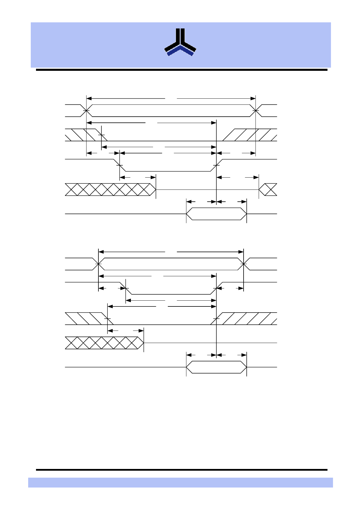
WRITE CYCLE 1 (WE# Controlled) (1,2,3,5,6)
Address
CE#
WE#
Dout
tWC
tAW
tCW
tAS
tWP
tWHZ
(4)
Din
tWR
TOW
High-Z
(4)
tDW
tDH
Data Valid
WRITE CYCLE 2 (CE# Controlled) (1,2,5,6)
Address
CE#
WE#
Dout
tAS
tWHZ
(4)
tWC
tAW
tCW
tWP
Din
tWR
High-Z
tDW
tDH
Data Valid
Notes :
1.WE#, CE# must be high during all address transitions.
2.A write occurs during the overlap of a low CE#, low WE#.
3.During a WE# controlled write cycle with OE# low, tWP must be greater than tWHZ + tDW to allow the drivers to turn off and data to be
placed on the bus.
4.During this period, I/O pins are in the output state, and input signals must not be applied.
5.If the CE# low transition occurs simultaneously with or after WE# low transition, the outputs remain in a high impedance state.
6.tOW and tWHZ are specified with CL = 5pF. Transition is measured ±500mV from steady state.
AUG09 v1.4
Alliance Memory Inc
Page 6 of 14
Share Link: 