AS6C4008 Просмотр технического описания (PDF) - Alliance Semiconductor
Номер в каталоге
Компоненты Описание
производитель
AS6C4008 Datasheet PDF : 14 Pages
| |||
$8*867 2009
AS6C4008
512K X 8 BIT LOW POWER CMOS SRAM
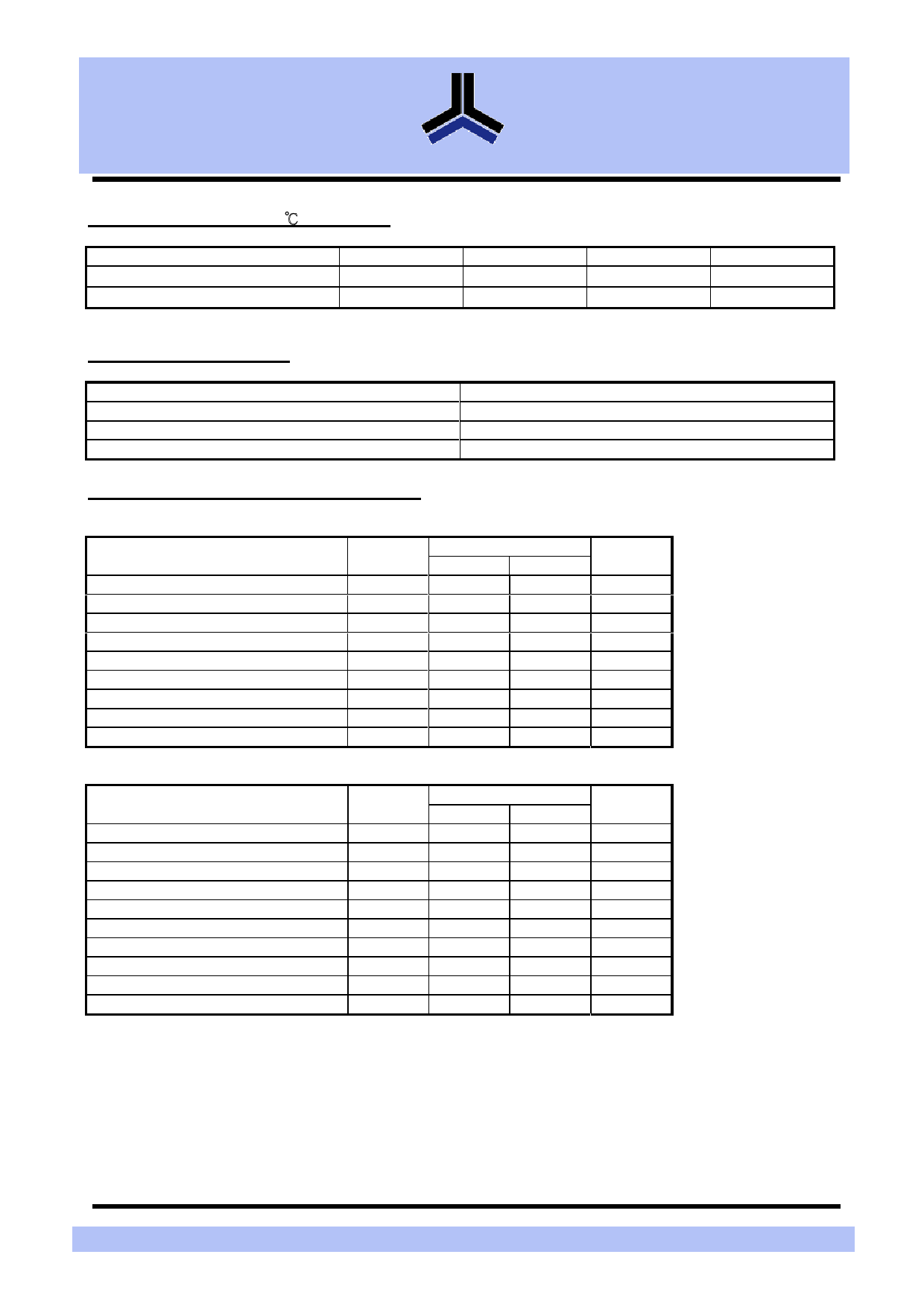
CAPACITANCE (TA = 25℃, f = 1.0MHz)
PARAMETER
SYMBOL
MIN.
Input Capacitance
CIN
-
Input/Output Capacitance
CI/O
-
Note : These parameters are guaranteed by device characterization, but not production tested.
MAX
6
8
AC TEST CONDITIONS
Input Pulse Levels
Input Rise and Fall Times
Input and Output Timing Reference Levels
Output Load
0.2V to VCC - 0.2V
3ns
1.5V
CL = 30pF + 1TTL, IOH/IOL = -2mA/4mA
AC ELECTRICAL CHARACTERISTICS
(1) READ CYCLE
PARAMETER
Read Cycle Time
Address Access Time
Chip Enable Access Time
Output Enable Access Time
Chip Enable to Output in Low-Z
Output Enable to Output in Low-Z
Chip Disable to Output in High-Z
Output Disable to Output in High-Z
Output Hold from Address Change
SYM.
t RC
tAA
tACE
tOE
tCLZ*
tOLZ*
tCHZ*
tOHZ*
tOH
AS6C4008-55
MIN.
MAX.
55
-
-
55
-
55
-
30
10
-
5
-
-
20
-
20
10
-
UNIT
ns
ns
ns
ns
ns
ns
ns
ns
ns
(2) WRITE CYCLE
PARAMETER
SYM.
AS6C4008-55
MIN.
MAX.
Write Cycle Time
tWC
55
-
Address Valid to End of Write
tAW
50
-
Chip Enable to End of Write
tCW
50
-
Address Set-up Time
tAS
0
-
Write Pulse Width
tWP
45
-
Write Recovery Time
tWR
0
-
Data to Write Time Overlap
tDW
25
-
Data Hold from End of Write Time
tDH
0
Output Active from End of Write
tOW*
5
-
Write to Output in High-Z
tWHZ*
-
20
*These parameters are guaranteed by device characterization, but not production tested.
UNIT
ns
ns
ns
ns
ns
ns
ns
ns
ns
ns
UNIT
pF
pF
AUG09 v1.4
Alliance Memory Inc
Page 4 of 14
Share Link: 