APT6013JFLL –Я—А–Њ—Б–Љ–Њ—В—А —В–µ—Е–љ–Є—З–µ—Б–Ї–Њ–≥–Њ –Њ–њ–Є—Б–∞–љ–Є—П (PDF) - Advanced Power Technology
–Э–Њ–Љ–µ—А –≤ –Ї–∞—В–∞–ї–Њ–≥–µ
–Ъ–Њ–Љ–њ–Њ–љ–µ–љ—В—Л –Ю–њ–Є—Б–∞–љ–Є–µ
–њ—А–Њ–Є–Ј–≤–Њ–і–Є—В–µ–ї—М
APT6013JFLL Datasheet PDF : 5 Pages
| |||
DYNAMIC CHARACTERISTICS
APT6013JFLL
Symbol Characteristic
Test Conditions
MIN TYP MAX UNIT
Ciss
Coss
Crss
Input Capacitance
Output Capacitance
Reverse Transfer Capacitance
VGS = 0V
VDS = 25V
f = 1 MHz
5630
1060
pF
70
Qg
Total Gate Charge 3
Qgs Gate-Source Charge
Qgd Gate-Drain ("Miller ") Charge
VGS = 10V
VDD = 300V
ID = 39A @ 25°C
130
25
nC
40
td(on)
tr
td(off)
tf
Eon
Eoff
Eon
Eoff
Turn-on Delay Time
Rise Time
Turn-off Delay Time
Fall Time
Turn-on Switching Energy 6
Turn-off Switching Energy
Turn-on Switching Energy 6
Turn-off Switching Energy
RESISTIVE SWITCHING
11
VGS = 15V
VDD = 300V
ID = 39A @ 25°C
13
ns
27
RG = 0.6вД¶
9
INDUCTIVE SWITCHING @ 25°C
VDD = 400V, VGS = 15V
575
ID = 39A, RG = 5вД¶
530
µJ
INDUCTIVE SWITCHING @ 125°C
VDD = 400V, VGS = 15V
935
ID = 39A, RG = 5вД¶
630
SOURCE-DRAIN DIODE RATINGS AND CHARACTERISTICS
Symbol Characteristic / Test Conditions
MIN TYP MAX UNIT
IS
Continuous Source Current (Body Diode)
ISM
Pulsed Source Current 1 (Body Diode)
39 Amps
156
VSD Diode Forward Voltage 2 (VGS = 0V, IS = -39A)
1.3 Volts
dv/dt Peak Diode Recovery dv/dt 5
15 V/ns
Reverse Recovery Time
trr
(IS = -39A, di/dt = 100A/µs)
Reverse Recovery Charge
Qrr
(IS = -39A, di/dt = 100A/µs)
Peak Recovery Current
IRRM
(IS = -39A, di/dt = 100A/µs)
Tj = 25°C
Tj = 125°C
Tj = 25°C
Tj = 125°C
Tj = 25°C
Tj = 125°C
250
ns
500
2.27
µC
6.87
14
Amps
22
THERMAL CHARACTERISTICS
Symbol Characteristic
MIN TYP MAX UNIT
RќЄJC
RќЄJA
Junction to Case
Junction to Ambient
0.27
40
°C/W
1 Repetitive Rating: Pulse width limited by maximum junction
temperature
2 Pulse Test: Pulse width < 380 µs, Duty Cycle < 2%
3 See MIL-STD-750 Method 3471
4 Starting Tj = +25¬∞C, L = 3.29mH, RG = 25вД¶, Peak IL = 39A
5 dv/dt numbers reflect the limitations of the test circuit rather than the
device itself. IS вЙ§ -ID39A di/dt вЙ§ 700A/¬µs VR вЙ§ VDSS TJ вЙ§ 150¬∞C
6 Eon includes diode reverse recovery. See figures 18, 20.
APT Reserves the right to change, without notice, the specifications and inforation contained herein.
0.30
0.25
0.9
0.20
0.7
0.15
0.10
0.05
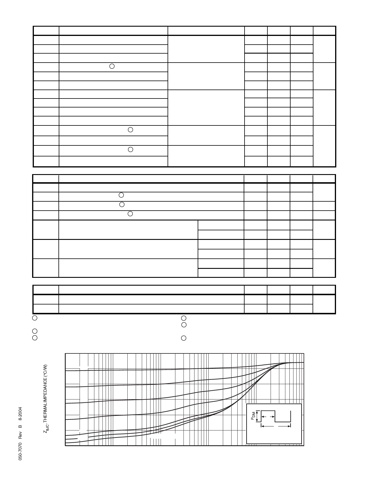
0
10-5
0.5
Note:
0.3
t1
0.1
0.05
SINGLE PULSE
t2
Duty Factor D = t1/t2
Peak TJ = PDM x ZќЄJC + TC
10-4
10-3
10-2
10-1
1
RECTANGULAR PULSE DURATION (SECONDS)
FIGURE 1, MAXIMUM EFFECTIVE TRANSIENT THERMAL IMPEDANCE, JUNCTION-TO-CASE vs PULSE DURATION
Share Link: 