LC8954 Просмотр технического описания (PDF) - SANYO -> Panasonic
Номер в каталоге
Компоненты Описание
производитель
LC8954 Datasheet PDF : 7 Pages
| |||
LC8954
Continued from preceding page.
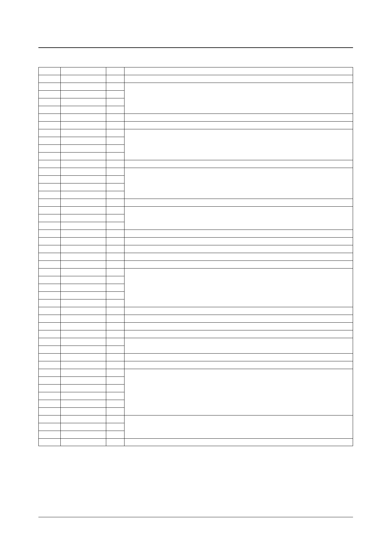
Pin No.
81
82
83
84
85
86
87
88
89
90
91
92
93
94
95
96
97
98
99
100
101
102
103
104
105
106
107
108
109
110
111
112
113
114
115
116
117
118
119
120
121
122
123
124
125
126
127
128
Pin
VSS
D1
D2
D3
D4
VSS
VDD
D5
D6
D7
D8
VSS
D9
D10
D11
D12
VSS
D13
D14
D15
ZHINT0
ZUDS
ZLDS
ZAS
ZCSCDIC
A1
A2
A3
A4
A5
R/W
ZDTACK
VDD
CPUCLK
CDPORT0
CDPORT1
ZHINT1
ZDONE
ZACK0
ZACK1
ZRDY0
ZRDY1
ZDRQ0
ZDRQ1
BUFFULL
DATAEMP
UNDFLOW
INIT
Type
P
B
B
B
B
P
P
B
B
B
B
P
B
B
B
B
P
B
B
B
O
I
I
I
I
I
I
I
I
I
I
B
P
I
B
B
O
B
I
I
O
O
O
O
O
O
O
I
Host CPU data bus
Type: I: Input pin, O: Output pin, B: Bi-directional pin, P: Power supply pin
Function
Host CPU data bus
Host CPU data bus
Host CPU data bus
Host CPU interrupt
High-order data strobe input
Low-order data strobe input
Address strobe signal
Chip select from the host CPU
Host CPU address
Read/write input
Data acknowledge signal
CPU clock input
General-purpose I/O signals
Host CPU interrupt
DMA transfer pin: Open drain with built-in pull-up resistors
For DMA transfer pins
SRAM status
Gain control register initialization input
No. 4127-6/7
Share Link: 