ADN4667 Просмотр технического описания (PDF) - Analog Devices
Номер в каталоге
Компоненты Описание
производитель
ADN4667 Datasheet PDF : 16 Pages
| |||
Data Sheet
FEATURES
±15 kV ESD protection on output pins
400 Mbps (200 MHz) switching rates
Flow through pinout simplifies PCB layout
300 ps typical differential skew
400 ps maximum differential skew
1.7 ns maximum propagation delay
3.3 V power supply
±310 mV differential signaling
Low power dissipation (10 mW typical)
Interoperable with existing 5 V LVDS receivers
High impedance on LVDS outputs on power-down
Conforms to TIA/EIA-644 LVDS standards
Industrial operating temperature range: −40°C to +85°C
Available in surface-mount (SOIC) and low profile
TSSOP package
Qualified for automotive applications
APPLICATIONS
Backplane data transmission
Cable data transmission
Clock distribution
GENERAL DESCRIPTION
The ADN4667 is a quad, CMOS, low voltage differential signaling
(LVDS) line driver offering data rates of over 400 Mbps (200 MHz)
and ultralow power consumption. It features a flow through
pinout for easy PCB layout and separation of input and output
signals.
The device accepts low voltage TTL/CMOS logic signals and
converts them to a differential current output of typically ±3.1 mA
for driving a transmission medium such as a twisted pair cable.
The transmitted signal develops a differential voltage of typi-
cally ±310 mV across a termination resistor at the receiving end.
This is converted back to a TTL/CMOS logic level by an LVDS
receiver, such as the ADN4668.
3 V LVDS Quad CMOS
Differential Line Driver
ADN4667
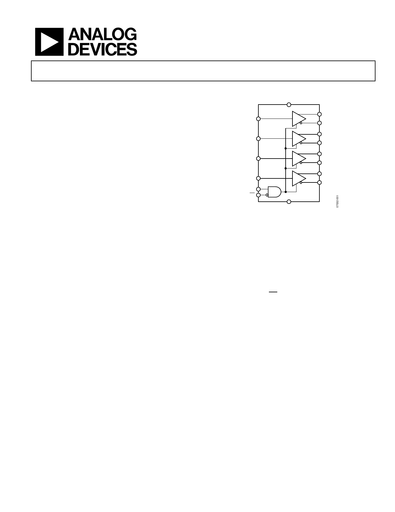
FUNCTIONAL BLOCK DIAGRAM
VCC
ADN4667
DIN1
D1
DOUT1+
DOUT1–
DIN2
DOUT2+
D2
DOUT2–
DIN3
DOUT3+
D3
DOUT3–
DIN4
EN
EN
DOUT4+
D4
DOUT4–
GND
Figure 1.
The ADN4667 also offers active high and active low enable/
disable inputs (EN and EN). These inputs control all four drivers
and turn off the current outputs in the disabled state to reduce
the quiescent power consumption to typically 10 mW.
The ADN4667 and its companion LVDS receiver, the ADN4668,
offer a new solution to high speed, point-to-point data trans-
mission, and a low power alternative to emitter-coupled logic
(ECL) or positive emitter-coupled logic (PECL).
Rev. B
Information furnished by Analog Devices is believed to be accurate and reliable. However, no
responsibility is assumed by Analog Devices for its use, nor for any infringements of patents or other
rights of third parties that may result from its use. Specifications subject to change without notice. No
license is granted by implication or otherwise under any patent or patent rights of Analog Devices.
Trademarks and registered trademarks are the property of their respective owners.
One Technology Way, P.O. Box 9106, Norwood, MA 02062-9106, U.S.A.
Tel: 781.329.4700
www.analog.com
Fax: 781.461.3113 ©2008–2012 Analog Devices, Inc. All rights reserved.
Share Link: 