MC141543 Просмотр технического описания (PDF) - Motorola => Freescale
Номер в каталоге
Компоненты Описание
производитель
MC141543 Datasheet PDF : 14 Pages
| |||
PIN DESCRIPTIONS
VSS(A) (Pin 1)
This pin provides the signal ground to the PLL circuitry.
Analog ground for PLL operation is separated from digital
ground for optimal performance.
VCO (Pin 2)
Pin 2 is a control voltage input to regulate an internal oscil-
lator frequency. See the Application Diagram for the applica-
tion values used.
RP (Pin 3)
An external RC network is used to bias an internal VCO to
resonate at the specific dot frequency. The maximum voltage
at Pin 3 should not exceed 3.5 V at any condition. See the
Application Diagram for the application values used.
VDD(A) (Pin 4)
Pin 4 is a positive 5 V supply for PLL circuitry. Analog pow-
er for PLL is separated from digital power for optimal perfor-
mance.
HFLB (Pin 5)
This pin inputs a negative polarity horizontal synchronize
signal pulse to phase lock an internal system clock gener-
ated by the on–chip VCO circuit.
SS (Pin 6)
This input pin is part of the SPI serial interface. An active
low signal generated by the master device enables this slave
device to accept data. This pin should be pulled high to termi-
nate the SPI communication. If M_BUS is employed as the
serial interface, this pin should be tied to either VDD or VSS.
SDA (MOSI) (Pin 7)
Data and control messages are being transmitted to this
chip from a host MCU via one of the two serial bus systems.
With either protocol, this wire is configured as a uni–direc-
tional data line. (Detailed description of these two protocols
will be discussed in the M_BUS and SPI sections).
SCL (SCK) (Pin 8)
A separate synchronizing clock input from the transmitter
is required for either protocol. Data is read at the rising edge
of each clock signal.
VDD (Pin 9)
This is the power pin for the digital logic of the chip.
VFLB (Pin 10)
Similar to Pin 5, this pin inputs a negative polarity vertical
synchronize signal pulse.
HTONE/PWMCK (Pin 11)
This is a multiplexed pin. When the PWMCK_EN bit is
cleared after power–on or by the MCU, this pin is HTONE
and outputs a logic high during windowing except when
graphics or characters are being displayed. It is used to low-
er the external R, G, and B amplifiers’ gain to achieve a
transparent windowing effect. If the PWMCK_EN bit is set to
1 via M_BUS or SPI, this pin is changed to a mode–depen-
dent clock output with 50/50 duty cycle and is synchronous
with the input horizontal synchronization signal at Pin 5. The
frequency is dependent on the mode in which the AMOSD is
currently running. The exact frequencies in the different reso-
lution modes are described in Table 1.
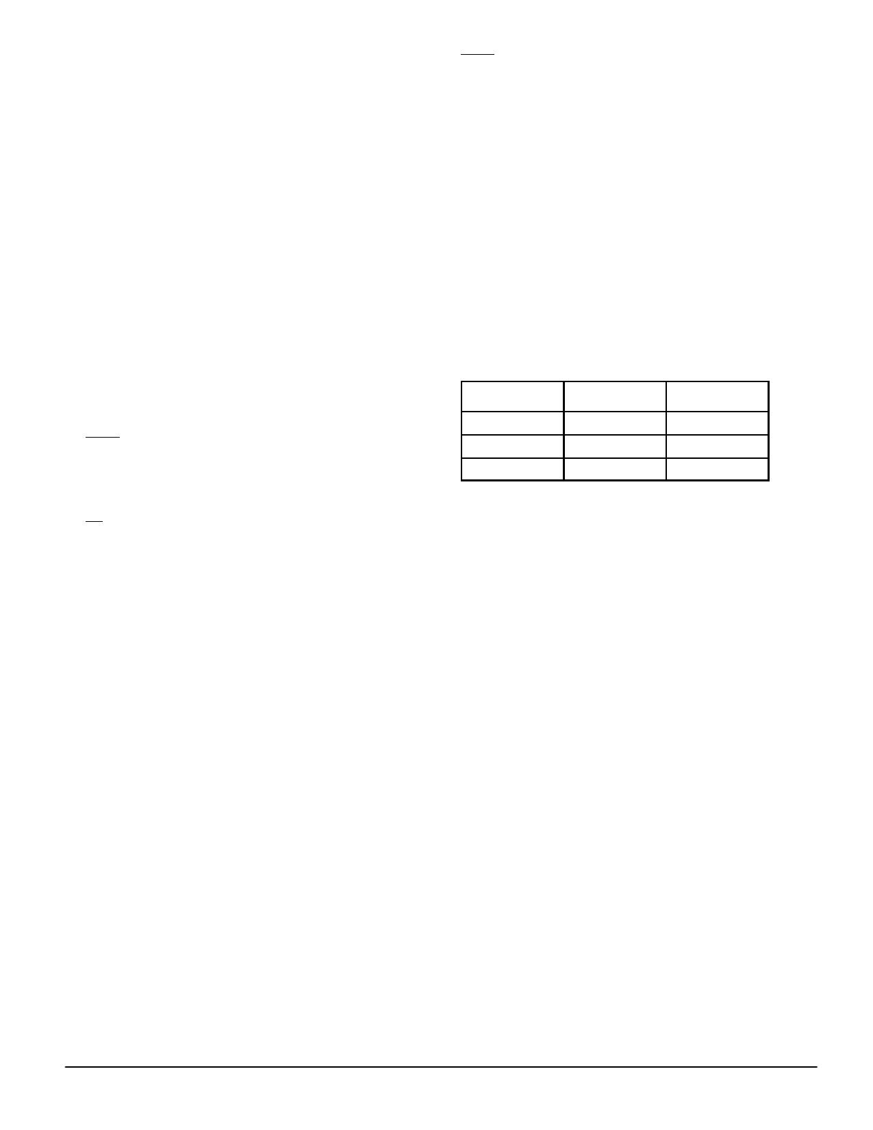
Table 1. PWM CLK Frequency
ÎÎÎÎÎÎÎÎÎÎÎÎÎÎÎ Resolution
ÎÎÎÎÎÎÎÎÎÎÎÎÎÎÎ 320 dots/line
ÎÎÎÎÎÎÎÎÎÎÎÎÎÎÎ 480 dots/line
ÎÎÎÎÎÎÎÎÎÎÎÎÎÎÎÎÎÎÎÎÎÎÎÎÎÎÎÎÎÎ 640 dots/line
Frequency
32 x Hf
48 x Hf
64 x Hf
Duty Cycle
50/50
50/50
50/50
NOTE: Hf is the frequency of the input H sync on Pin 5.
Typically, this clock is fed into an external pulse width mod-
ulation module as its clock source. Because of the synchro-
nization between PWM clock and H sync, a better
performance on the PWM controlled functions can be
achieved.
FBKG (Pin 12)
This pin outputs a logic high while displaying characters or
windows when the FBKGC bit in the frame control register is
0, and output a logic high only while displaying characters
when the FBKGC bit is 1. It is defaulted to high–impedance
state after power–on, or when there is no output. An external
10 kΩ resistor pulled low is recommended to avoid level tog-
gling caused by hand effect when there is no output.
B,G,R (Pins 13,14,15)
AMOSD color output is TTL level RGB to the host monitor.
These three signals are active high output pins that are in a
high–impedance state when AMOSD is disabled.
VSS (Pin 16)
This is the ground pin for the digital logic of the chip.
MC141543
4
MOTOROLA
Share Link: 