AD75004 Просмотр технического описания (PDF) - Analog Devices
Номер в каталоге
Компоненты Описание
производитель
AD75004 Datasheet PDF : 4 Pages
| |||
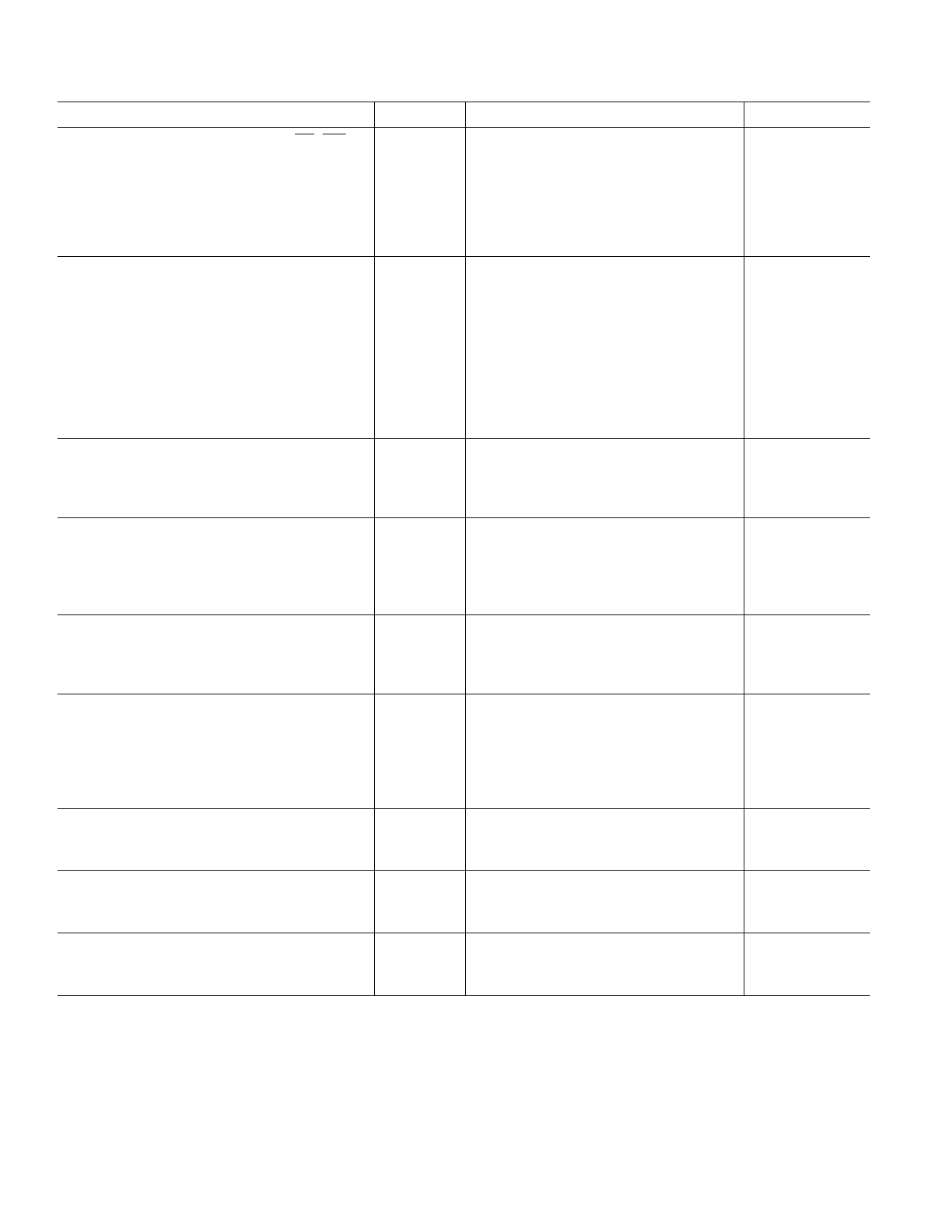
AD75004–SPECIFICATIONS (TA = +25؇C, ؎12.0 V power supplies unless otherwise noted)
Parameter
Symbol
Min
Typ
Max
Units
DIGITAL INPUTS (D0–D7, A0–A3, CS, WR)
Logic Levels (TTL Compatible)
Input Voltage, Logic “1”
VIH
Input Voltage, Logic “0”
VIL
Input Current, VIH = 5.5 V
IIH
Input Current, VIL = 0.8 V
IIL
Input Capacitance
CIN
ACCURACY
Resolution
Integral Linearity Error
Integral Linearity Error, TMIN to TMAX
Differential Linearity Error
Differential Linearity Error, TMIN to TMAX
Gain (Full-Scale) Error1
Gain Error Drift, TMIN to TMAX1
Bipolar Zero Error1
Bipolar Zero Error Drift, TMIN to TMAX1
CHANNEL-TO-CHANNEL MISMATCH
Integral Linearity Error
Gain Error1
Bipolar Zero Error1
2.0
5.5
0
0.8
10
10
10
12
± 1/4
؎1/2
± 1/2
± 3/4
± 1/2
؎3/4
Guaranteed Monotonic
±2
؎10
± 15
± 30
±1
؎2
±3
±7
± 1/2
؎1
±1
؎4
±1
؎2
V
V
µA
µA
pF
Bits
LSB
LSB
LSB
LSB
ppm/°C
LSB
ppm/°C
LSB
LSB
LSB
DYNAMIC PERFORMANCE
Settling Time to ± 0.01% of FSR
for FSR Change, 2 kΩ || 500 pF Load
Slew Rate, 2 kΩ || 500 pF Load
Digital Input Crosstalk (Static)2
2
4
µs
5
V/µs
–50
dB
ANALOG OUTPUTS
Full-Scale Range (FSR)
Output Current
Short Circuit Limit Current
VOUT
±5
V
IOUT
±5
mA
؎40
mA
VOLTAGE REFERENCE
Reference Output Voltage
Temperature Coefficient
Reference Output Currents3
Reference Input Voltage
Reference Input Current @ 5.0 V
VREFOUT
VREFIN
IREFIN
4.97
3.0
4.5
5.00
± 15
5.0
5.0
5.03
± 25
5.5
3.0
V
ppm/°C
mA
V
mA
POWER SUPPLY GAIN SENSITIVITY
∆Gain/∆VDD, VDD = +10.8 to +13.2 V dc1
∆Gain/∆VSS, VSS = –10.8 to –13.2 V dc1
± 15
؎25
ppm of FSR/%
± 15
؎25
ppm of FSR/%
POWER SUPPLY REQUIREMENTS
Voltage Range
Supply Currents
TEMPERATURE RANGE
Specification
Storage
VDD, VSS
؎10.8
± 12
IDD, ISS
± 25
TMIN, TMAX 0
–65
؎13.2
V
؎30
mA
+70
°C
+150
°C
NOTES
1Gain and bipolar zero errors are measured using internal voltage reference and include its errors.
2Digital crosstalk is defined as the change in any one output’s steady state value as a result of any other output being driven from VOUTMIN to VOUTMAX into a
2 kΩ || 500 pF load by means of varying the digital input code.
3The internal voltage reference is intended to drive on-chip only; buffer it if using it externally.
4All minimum and maximum specifications are guaranteed, and specifications shown in boldface are tested on all production units at final electrical test. Results from
those tests are used to calculate outgoing quality levels.
Specifications subject to change without notice.
–2–
REV. A
Share Link: 