3D7622 Просмотр технического описания (PDF) - Data Delay Devices
Номер в каталоге
Компоненты Описание
производитель
3D7622 Datasheet PDF : 7 Pages
| |||
APPLICATION NOTES (CONT’D)
3D7622
TRIGGER & RESET TIMING
Figure 2 shows the timing diagram of the device
when the reset input (RES) is not used. In this
case, the pulse is triggered by the rising edge of
the TRIG signal and ends at a time determined
by the address loaded into the device. While the
pulse is active, any additional triggers occurring
are ignored. Once the pulse has ended, and after
a short recovery time, the next trigger is
recognized. Figure 3 shows the timing for the
case where a reset is issued before the pulse
has ended. Again, there is a short recovery time
required before the next trigger can occur.
ADDRESS UPDATE
While observing data setup (tDS) and data hold
(tDH) requirements, timing data is loaded in MSB-
to-LSB order by the rising edge of the clock (SC)
while the enable (AE) is high, as shown in Figure
4. The falling edge of the AE activates the new
pulse width value, which is reflected at the output
upon the next trigger.
As shown in the figure, most of the address
information for the next pulse can be loaded
while the current pulse is active. It is only on the
falling-edge of AE that the device adjusts to the
new pulse width setting. In other words, the
device controller does not need to wait for the
current pulse to end before beginning an address
update sequence. This can save a considerable
amount of time in certain applications.
As data is shifted into the serial data input (SI),
the previous contents of the 22-bit input register
are shifted out of the serial output pin (SO) in
MSB-to-LSB order. This allows cascading of
multiple devices by connecting SO of the
preceding device to SI of the succeeding device,
as illustrated in Figure 5. The total number of
serial data bits in a cascade configuration must
be 22 times the number of units, and each group
of 22 bits must be transmitted in MSB-to-LSB
order.
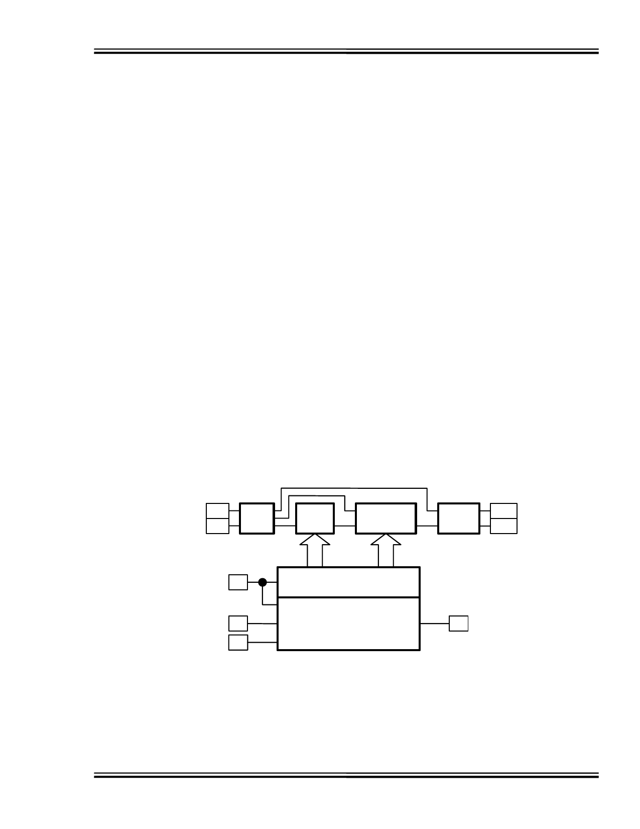
TRIGGER TRG
RESET RES
INPUT
LOGIC
ADDR ENABLE AE
DELAY
LINE
OSCILLATOR/
COUNTER
6
16
LSB
MSB
22-BIT LATCH
OUTPUT
LOGIC
OUT
OUTB
PULSE OUT
SERIAL IN SI
SERIAL CLK SC
22-BIT INPUT
REGISTER
SO SERIAL OUT
Figure 1: Functional block diagram
Doc #06007
DATA DELAY DEVICES, INC.
3
5/8/2006
3 Mt. Prospect Ave. Clifton, NJ 07013
Share Link: 