VSC7130(2000) Просмотр технического описания (PDF) - Vitesse Semiconductor
Номер в каталоге
Компоненты Описание
производитель
VSC7130 Datasheet PDF : 22 Pages
| |||
VITESSE
SEMICONDUCTOR CORPORATION
Advance Product Information
VSC7130
Dual Repeater/Retimer
for Fibre Channel and Gigabit Ethernet
DC Characteristics (Over recommended operating conditions).
Parameters
Description
Min Typ Max Units
VIH
VIL
IIH
IIL
VOH
VOL
VDD
PD
IDD
∆VIN1
Input HIGH voltage (TTL)
2.0 — 5.5
V
Input LOW voltage (TTL)
0
— 0.8
V
Input HIGH current (TTL)
— 50 500
µA
Input LOW current (TTL)
—
— -500
µA
Output HIGH Voltage (TTL)
2.4 — —
V
Output LOW Voltage (TTL)
— — 0.5
V
Supply voltage
3.14 — 3.47
V
Power Dissipation
— 500 800 mW
Supply current
— 150 230
mA
PECL input swing: RX0, RX1 or SI
(PECL+) - (PECL-)
300
— 2200 mVp-p
∆VOUT751
PECL output swing: TX or SO
(PECL+) - (PECL-)
1200 — 2200 mVp-p
∆VOUT501
PECL output swing: TX or SO
(PECL+) - (PECL-)
1000 — 2200 mVp-p
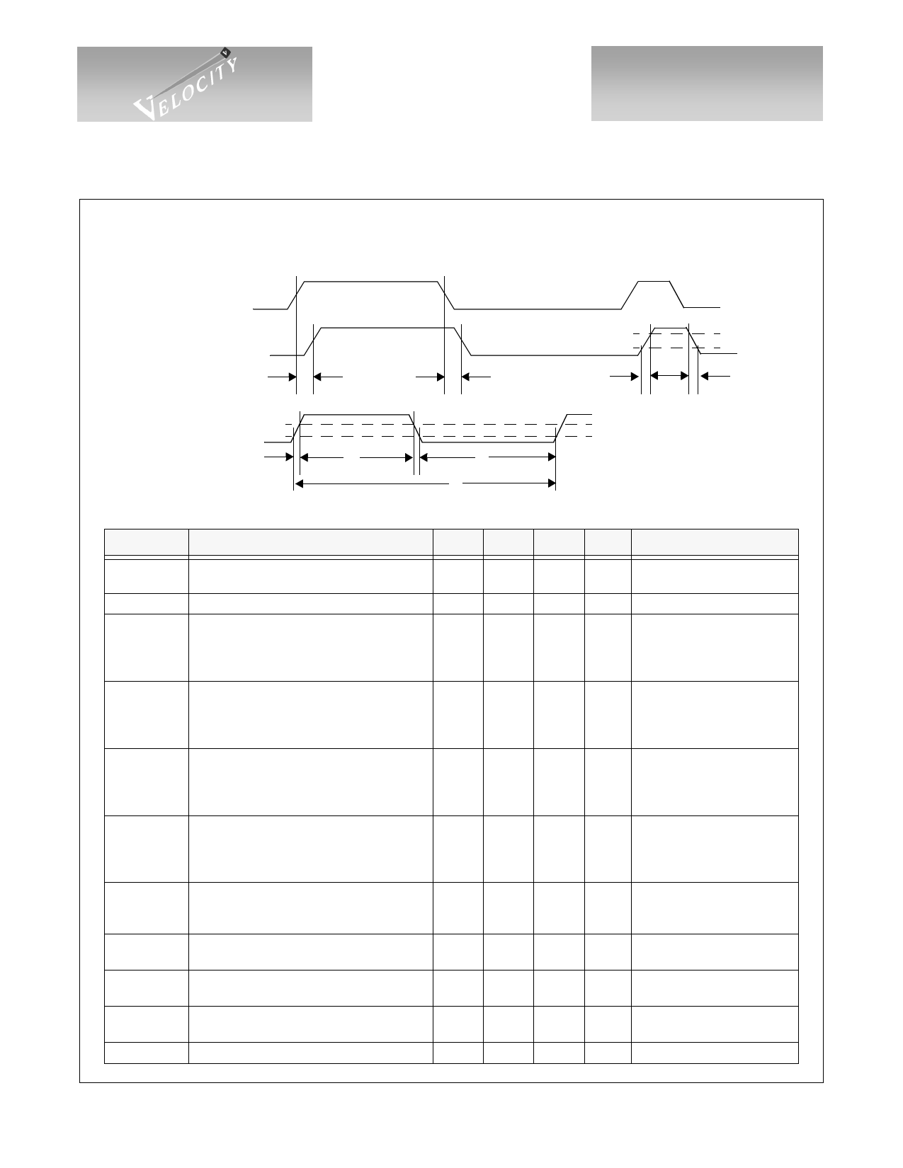
1 NOTE: Refer to Application Note, AN-37, for differential measurement techniques.
Conditions
—
VIN = 2.4 V
VIN = 0.5 V
IOH = -1.0mA
IOL= +1.0mA
VDD = 3.3V + 5%
Outputs open, VDD = VDD max
Outputs open, VDD = VDD max
AC Coupled.
Internally biased at VDD/2
75Ω to VDD – 2.0 V
50Ω to VDD – 2.0 V
Absolute Maximum Ratings (1)
Power Supply Voltage (VDD) .............................................................................................................-0.5V to +4V
PECL DC Input Voltage ......................................................................................................... -0.5V to VDD +0.5V
TTL DC Input Voltage....................................................................................................................... -0.5V to 5.5V
DC Voltage Applied to TTL Outputs ................................................................................... -0.5V to VDD + 0.5V
TTL Output Current ..................................................................................................................................+/-50mA
PECL Output Current ................................................................................................................................+/-50mA
Case Temperature Under Bias .........................................................................................................-55° to +125oC
Storage Temperature.......................................................................................................................-65° to + 150oC
Maximum Input ESD (Human Body Model).............................................................................................. 1500 V
Recommended Operating Conditions
Power Supply Voltage.................................................................................................... ....... ...... ........3.3V +/- 5%
Ambient Operating Temperature Range............................................................... 0°C Ambient to +95°C Case
Notes:
1) CAUTION: Stresses listed under “Absolute Maximum Ratings” may be applied to devices one at a time without causing per-
manent damage. Functionality at or above the values listed is not implied. Exposure to these values for extended periods
may affect device reliability.
G52297-0, Rev. 2.3
1/17/00
© VITESSE SEMICONDUCTOR CORPORATION
741 Calle Plano, Camarillo, CA 93012 • 805/388-3700 • FAX: 805/987-5896
Page 15
Share Link: 