CY7C1061DV18-15BV1XI –Я—А–Њ—Б–Љ–Њ—В—А —В–µ—Е–љ–Є—З–µ—Б–Ї–Њ–≥–Њ –Њ–њ–Є—Б–∞–љ–Є—П (PDF) - Cypress Semiconductor
–Э–Њ–Љ–µ—А –≤ –Ї–∞—В–∞–ї–Њ–≥–µ
–Ъ–Њ–Љ–њ–Њ–љ–µ–љ—В—Л –Ю–њ–Є—Б–∞–љ–Є–µ
–њ—А–Њ–Є–Ј–≤–Њ–і–Є—В–µ–ї—М
CY7C1061DV18-15BV1XI Datasheet PDF : 18 Pages
| |||
CY7C1061DV18
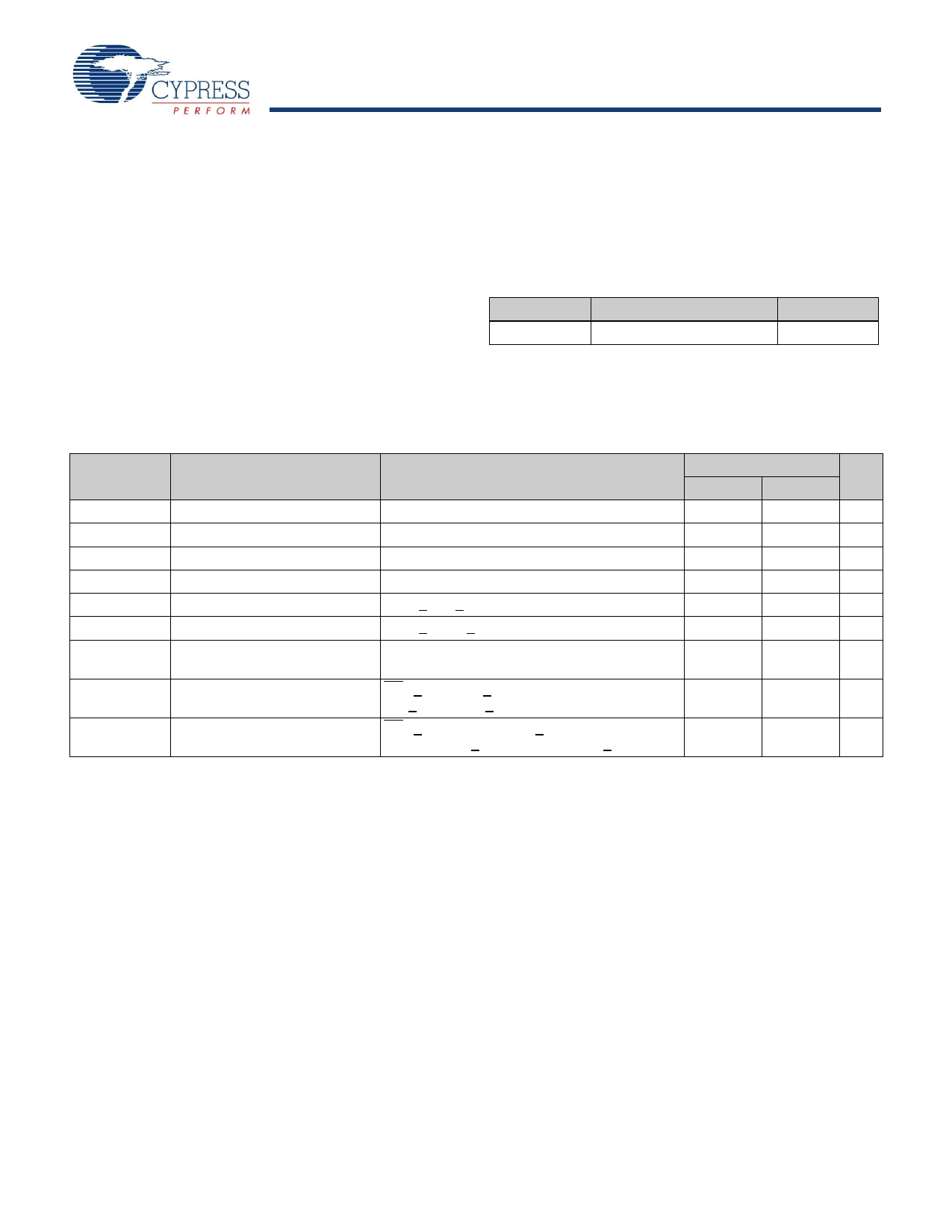
Maximum Ratings
Exceeding maximum ratings may impair the useful life of the
device. These user guidelines are not tested.
Storage temperature ................................ вАУ65 пВ∞C to +150 пВ∞C
Ambient temperature with
power applied .......................................... вАУ55 пВ∞C to +125 пВ∞C
Supply voltage on
VCC to relative GND [1] ..............................вАУ0.2 V to +2.45 V
DC voltage applied to outputs
in High Z state [1] .......................................вАУ0.2 V to +2.45 V
DC input voltage [1] ....................................вАУ0.2 V to +2.45 V
Current into outputs (LOW) ........................................ 20 mA
Static discharge voltage
(per MIL-STD-883, method 3015) ........................... >2001 V
Latch-up current ..................................................... >200 mA
Operating Range
Range
Industrial
Ambient Temperature
вАУ40 пВ∞C to +85 пВ∞C
VCC
1.7 V to 2.2 V
DC Electrical Characteristics
Over the Operating Range
Parameter
Description
VOH
Output HIGH voltage
VOL
Output LOW voltage
VIH
Input HIGH voltage
VIL
Input LOW voltage[1]
IIX
Input leakage current
IOZ
Output leakage current
ICC
VCC operating supply current
ISB1
Automatic CE power-down
current вАУ TTL inputs
ISB2
Automatic CE power-down
current вАУ CMOS inputs
Test Conditions
Min VCC, IOH = вАУ0.1 mA
Min VCC, IOL = 0.1 mA
GND < VIN < VCC
GND < VOUT < VCC, output disabled
Max VCC, f = fMAX = 1/tRC,
IOUT = 0 mA CMOS levels
CE1 > VIH, CE2 < VIL, Max VCC,
VIN > VIH or VIN < VIL, f = fMAX
CE1 > VCC вАУ 0.2 V, CE2 < 0.2 V,
Max VCC, VIN > VCC вАУ 0.2 V, or VIN < 0.2 V, f = 0
-15
Unit
Min
Max
1.4
вАУ
V
вАУ
0.2
V
1.4
вАУ0.2
VCC + 0.2 V
0.4
V
вАУ1
+1
пБ≠A
вАУ1
+1
пБ≠A
вАУ
150
mA
вАУ
30
mA
вАУ
25
mA
Note
1. VIL (min) = вАУ2.0 V for pulse durations of less than 20 ns.
Document Number: 001-08350 Rev. *I
Page 5 of 18
Share Link: 