CY7C1061DV18-15BV1XI –ü—Ä–ĺ—Ā–ľ–ĺ—ā—Ä —ā–Ķ—Ö–Ĺ–ł—á–Ķ—Ā–ļ–ĺ–≥–ĺ –ĺ–Ņ–ł—Ā–į–Ĺ–ł—Ź (PDF) - Cypress Semiconductor
–Ě–ĺ–ľ–Ķ—Ä –≤ –ļ–į—ā–į–Ľ–ĺ–≥–Ķ
–ö–ĺ–ľ–Ņ–ĺ–Ĺ–Ķ–Ĺ—ā—č –ě–Ņ–ł—Ā–į–Ĺ–ł–Ķ
–Ņ—Ä–ĺ–ł–∑–≤–ĺ–ī–ł—ā–Ķ–Ľ—Ć
CY7C1061DV18-15BV1XI Datasheet PDF : 18 Pages
| |||
CY7C1061DV18
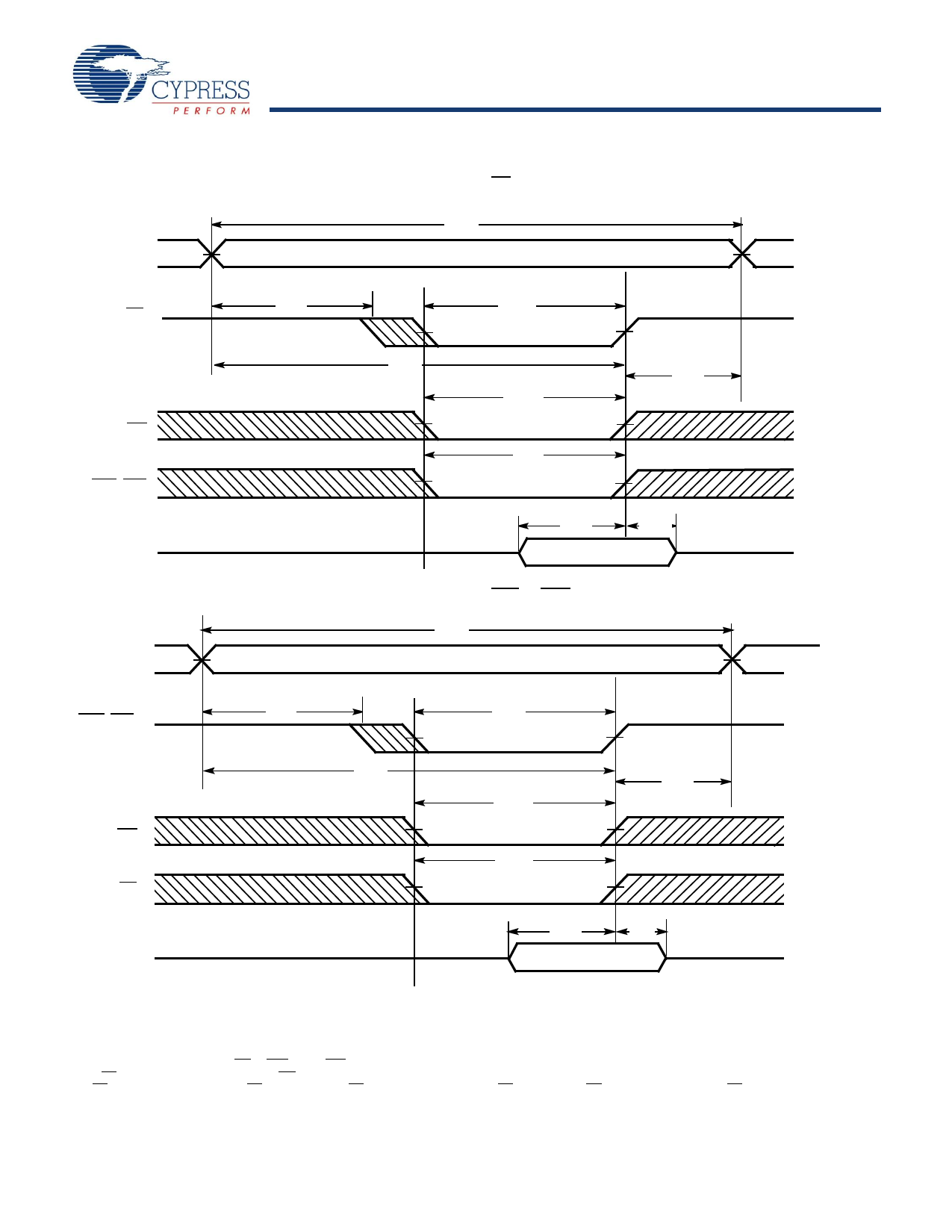
Switching Waveforms(continued)
Figure 7. Write Cycle No. 1 (CE Controlled) [18, 19, 20]
tWC
ADDRESS
CE
WE
BHE, BLE
DATA I/O
ADDRESS
tSA
tSCE
tAW
tHA
tPWE
tBW
tSD
tHD
DATA IN VALID
Figure 8. Write Cycle No. 2 (BLE or BHE Controlled)
tWC
BHE, BLE
WE
CE
DATA I/O
tSA
tAW
tBW
tHA
tPWE
tSCE
tSD
tHD
DATA IN VALID
Notes
18. Data I/O is high impedance if OE or BHE and/or BLE = VIH.
19. If CE1 goes HIGH simultaneously with WE going HIGH, the output remains in a high impedance state.
20. CE is the logical combination of CE1 and CE2. When CE1 is LOW and CE2 is HIGH, CE is LOW; when CE1 is HIGH or CE2 is LOW, CE is HIGH.
Document Number: 001-08350 Rev. *I
Page 10 of 18
Share Link: 