SY89423V Просмотр технического описания (PDF) - Micrel
Номер в каталоге
Компоненты Описание
производитель
SY89423V Datasheet PDF : 8 Pages
| |||
Micrel
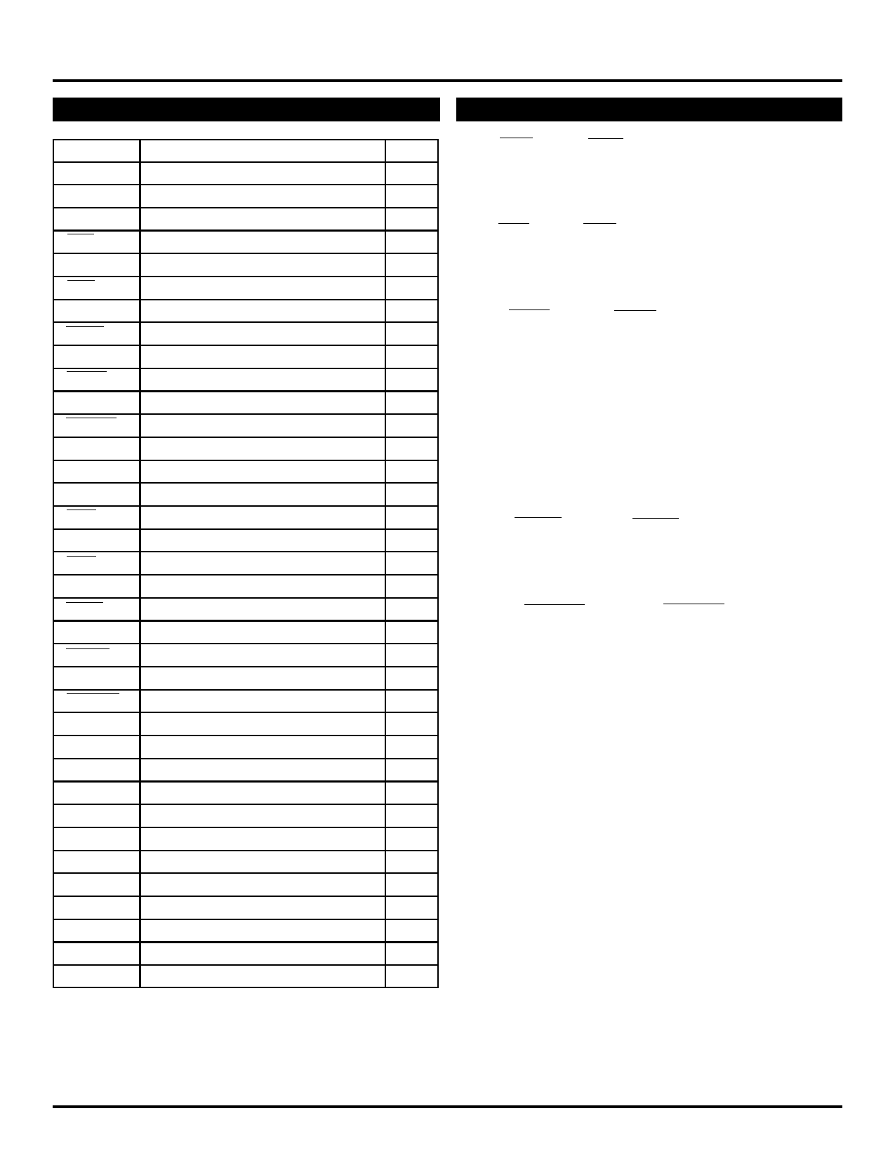
PIN NAMES
Pin
F1A
F2A
RINA
RINA
FINA
FINA
HFINA
HFINA
FOUTA
FOUTA
HFOUTA
HFOUTA
F1B
F2B
RINB
RINB
FINB
FINB
HFINB
HFINB
FOUTB
FOUTB
HFOUTB
HFOUTB
VCC
VCCOA
VCCOB
VEE
S1A
S2A
S3A
S1B
S2B
S3B
S4B
S5B
Function
Filter Pin 1A
Filter Pin 2A
Inverted Reference Input A
Reference Input A
Feedback Input A
Inverted Feedback Input A
High Frequency Input A
Inverted High Frequency Input A
Frequency Output A
Inverted Frequency Output A
High Frequency Output A
Inverted High Frequency Output A
Filter Pin 1B
Filter Pin 2B
Reference Input B
Inverted Reference Input B
Feedback Input B
Inverted Feedback Input B
High Frequency Input B
Inverted High Frequency Input B
Frequency Output B
Inverted Frequency Output B
High Frequency Output B
Inverted Frequency Output B
VCC
Output VCC
Output VCC
VEE (0V)
Select Input 1A (TTL)
Select Input 2A (TTL)
Select Input 3A (TTL)
Select Input 1B (TTL)
Select Input 2B (TTL)
Select Input 3B (TTL)
Select Input 4B (TTL)
Select Input 5B (TTL)
Precision Edge®
SY89423V
PIN DESCRIPTION
I/O
RINA, RINA, RINB, RINB
I/O
Reference frequency inputs for loop A and B. These are
differential signal pairs and may be driven differentially or
I/O single-ended.
I
FINA, FINA, FINB, FINB
I
Feedback frequency inputs for loop A and B. These are
I
differential signal pairs and may be driven differentially or
I
single-ended.
I
HFINA, HFINA, HFINB, HFINB
I
High frequency feedback inputs. Differential drive is
O
recommended.
O
F1A, F2A, F1B, F2B
O
These pins are connection points for the loop filters, which are
O
to be provided off-chip. F1X is the high impedance side, F2X
I/O
is the reference side. The loop filter should be a first order, low
pass with a DC block. The difference voltage on these pins will
I/O be a DC level, which is controlled by the loop feedback and
I
determined by the required VCO frequency.
I
FOUTA, FOUTA, FOUTB, FOUTB
I
Frequency outputs for the loops. These are differential, positive
I
referenced, emitter-follower signals and must be terminated
I
off-chip. Termination in 50 ohms is recommended.
I
HFOUTA, HFOUTA, HFOUTB, HFOUTB
O
High frequency outputs. These are differential, positive
O
referenced, emitter-follower signals and must be terminated
off-chip. Termination in 50 ohms is recommended.
O
O
S1A, S2A, S3A, S1B, S2B, S3B, S4B, S5B
—
These inputs are used to select the configuration for PLLA and
PLLB. See the Frequency Selection Table for details of the
—
logic.
—
—
VCC
This is the positive supply for the chip. It should be decoupled
I
and present a low impedance in order to assure low-jitter
I
operation.
I
VCCOA, VCCOB
I
These are the positive supplies for the output buffers. They are
I
constrained to be equal to or less than the value of VCC.
I
VEE
I
This pin is the negative supply for the chip and is normally
I
connected to ground (0V).
M9999-091707
hbwhelp@micrel.com or (408) 955-1690
3
Share Link: 