EVAL-AD5761RSDZ(RevA) –Я—А–Њ—Б–Љ–Њ—В—А —В–µ—Е–љ–Є—З–µ—Б–Ї–Њ–≥–Њ –Њ–њ–Є—Б–∞–љ–Є—П (PDF) - Analog Devices
–Э–Њ–Љ–µ—А –≤ –Ї–∞—В–∞–ї–Њ–≥–µ
–Ъ–Њ–Љ–њ–Њ–љ–µ–љ—В—Л –Ю–њ–Є—Б–∞–љ–Є–µ
–њ—А–Њ–Є–Ј–≤–Њ–і–Є—В–µ–ї—М
EVAL-AD5761RSDZ
(Rev.:RevA)
(Rev.:RevA)
Analog Devices

EVAL-AD5761RSDZ Datasheet PDF : 35 Pages
| |||
AD5761R/AD5721R
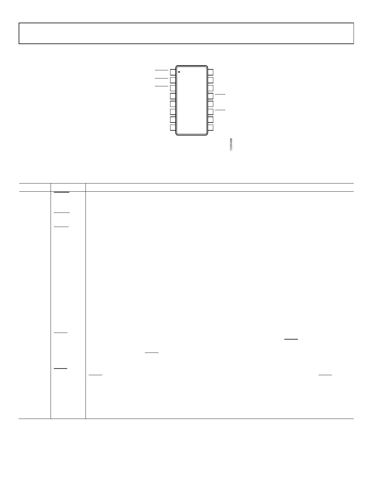
PIN CONFIGURATIONS AND FUNCTION DESCRIPTIONS
ALERT 1
CLEAR 2
RESET 3
VREFIN/VREFOUT 4
AGND 5
VSS 6
VOUT 7
VDD 8
AD5761R/
AD5721R
TOP VIEW
(Not to Scale)
16 DGND
15 DVCC
14 SCLK
13 SYNC
12 SDI
11 LDAC
10 SDO
9 DNC
NOTES
1. DNC = DO NOT CONNECT. DO NOT CONNECT
TO THIS PIN.
Figure 5. 16-Lead TSSOP Pin Configuration
Data Sheet
Table 5. 16-Lead TSSOP Pin Function Descriptions
Pin No. Mnemonic Description
1
ALERT
Active Low Alert. This pin is asserted low when the die temperature exceeds approximately 150°C, or when an
output short circuit or a brownout occurs. This pin is also asserted low during power-up, a full software reset, or
a hardware reset, for which a write to the control register asserts the pin high.
2
CLEAR
Falling Edge Clear Input. Asserting this pin sets the DAC register to zero scale, midscale, or full-scale code (user
selectable) and updates the DAC output. This pin can be left floating because there is an internal pull-up resistor.
3
RESET
Active Low Reset Input. Asserting this pin returns the AD5761R/AD5721R to their default power-on status
where the output is clamped to ground and the output buffer is powered down. This pin can be left floating
because there is an internal pull-up resistor.
4
VREFIN/VREFOUT Internal Reference Voltage Output and External Reference Voltage Input. For specified performance,
VREFIN/VREFOUT = 2.5 V. Connect a 10 nF capacitor with the internal reference to minimize the noise.
5
AGND
Ground Reference Pin for Analog Circuitry.
6
VSS
Negative Analog Supply Connection. A voltage in the range of вИТ16.5 V to 0 V can be connected to this pin. For
unipolar output ranges, connect this pin to 0 V. VSS must be decoupled to AGND.
7
VOUT
Analog Output Voltage of the DAC. The output amplifier is capable of directly driving a 2 kќ©, 1 nF load.
8
VDD
Positive Analog Supply Connection. A voltage in the range of 4.75 V to 30 V can be connected to this pin for
unipolar output ranges. Bipolar output ranges accept a voltage in the range of 4.75 V to 16.5 V. VDD must be
decoupled to AGND.
9
DNC
Do Not Connect. Do not connect to this pin.
10
SDO
Serial Data Output. This pin clocks data from the serial register in daisy-chain or readback mode. Data is clocked
out on the rising edge of SCLK and is valid on the falling edge of SCLK.
11
LDAC
Load DAC. This logic input updates the DAC register and, consequently, the analog output. When tied
permanently low, the DAC register is updated when the input register is updated. If LDAC is held high during
the write to the input register, the DAC output register is not updated, and the DAC output update is held off
until the falling edge of LDAC. This pin can be left floating because there is an internal pull-up resistor.
12
SDI
Serial Data Input. Data must be valid on the falling edge of SCLK.
13
SYNC
Active Low Synchronization Input. This pin is the frame synchronization signal for the serial interface. While
SYNC is low, data is transferred in on the falling edge of SCLK. Data is latched on the rising edge of SYNC.
14
SCLK
Serial Clock Input. Data is clocked into the input shift register on the falling edge of SCLK. This pin operates at
clock speeds of up to 50 MHz.
15
DVCC
Digital Supply. The voltage range is from 1.7 V to 5.5 V. The applied voltage sets the voltage at which the digital
interface operates.
16
DGND
Digital Ground.
Rev. A | Page 10 of 35
Share Link: