MCP6N16-010E Просмотр технического описания (PDF) - Microchip Technology
Номер в каталоге
Компоненты Описание
производитель
MCP6N16-010E Datasheet PDF : 58 Pages
| |||
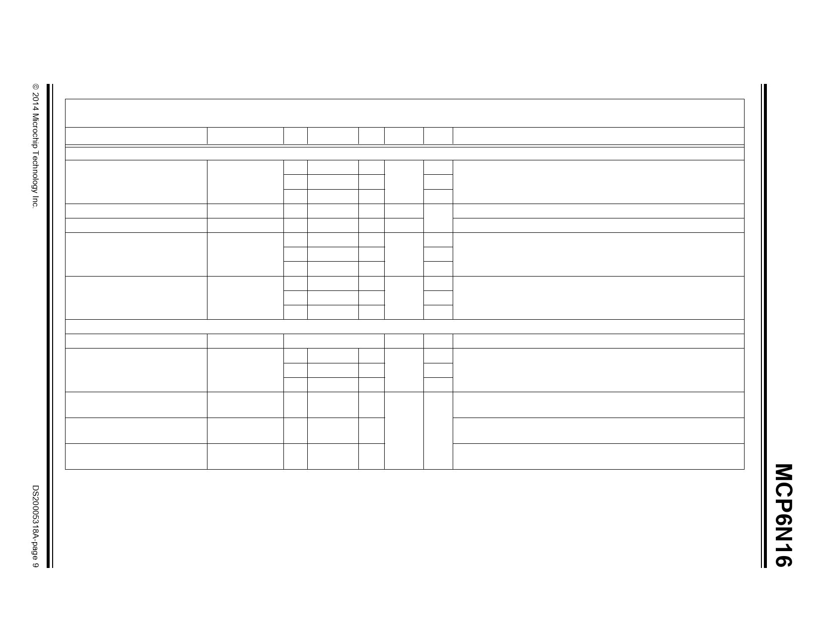
TABLE 1-2: AC ELECTRICAL SPECIFICATIONS
Electrical Characteristics: Unless otherwise indicated, TA = +25°C, VDD = 1.8V to 5.5V, VSS = GND, VCM = VDD/2, VDM = 0V, VREF = VDD/2, VL = VDD/2,
RL = 10 kΩ to VL, CL = 60 pF, GDM = GMIN and EN = VDD; see Figures 1-7 and 1-8.
Parameters
Sym.
Min. Typ. Max. Units GMIN
Conditions
AC Response
Gain-Bandwidth Product
GBWP
—
0.5
— MHz 1
—
5
—
10
—
35
—
100
Phase Margin
PM
—
70
—
°
all
Open-Loop Output Impedance
Power Supply Rejection Ratio
ROL
PSRR
—
1.6
— kΩ
—
80
— dB
1 f = 1 kHz
—
98
—
10
—
123
—
100
Common Mode Rejection Ratio CMRR, CMRR2 —
83
— dB
1 f = 10 kHz
at VCM and VREF
—
80
—
10
—
140
—
100
Step Response (see Section 4.1.4 “AC Performance”)
Slew Rate
SR
Note 1
V/µs all
Start-Up Time
tSTR
—
2
— ms
1 GDM = 1000, VDD power up to 0.1% VOUT settling (Note 3, Note 4)
—
0.3
—
10
—
0.2
—
100
Overdrive Recovery,
Input Common Mode
tIRC
—
1
—
µs
all VIP =VIM = VIVH + 0.5V to VDD – 1V (or VIVL – 0.5V to 1V),
90% of VOUT change (IB ≤ 2 mA) (Note 4)
Overdrive Recovery,
Input Differential Mode
tIRD
—
10
—
GMINVDM = GMINVDMH + 0.5V to 0V (or GMINVDML – 0.5V to 0V),
VREF = 1V (or VDD – 1V), 90% of VOUT change (Note 4)
Overdrive Recovery, Output
tOR
—
180
—
GDMVDM = 1.5V to 0V (or -1.5V to 0V),
VREF = VDD – 1V (or 1V), 90% of VOUT change (Note 4)
Note 1: The slew rate is limited by the GBWP; the large signal step response is dominated by the small signal bandwidth.
2: These parameters were characterized using the circuit in Figure 1-8. In Figures 2-75 and 2-76, there is an IMD tone at DC, a residual tone at 100 Hz and
other IMD tones and clock tones.
3: High gains behave differently; see Section 4.4.4 “Offset at Power-Up”.
4: tSTR, tSTL, tIRC, tIRD and tOR include some uncertainty due to clock edge timing.
Share Link: 