MC74ACT153DTR2 Просмотр технического описания (PDF) - ON Semiconductor
Номер в каталоге
Компоненты Описание
производитель
MC74ACT153DTR2 Datasheet PDF : 6 Pages
| |||
MC74AC153 MC74ACT153
FUNCTIONAL DESCRIPTION
The MC74AC153/74ACT153 is a dual 4-input multiplexer.
It can select two bits of data from up to four sources under the
control of the common Select inputs (S0, S1). The two 4-input
multiplexer circuits have individual active-LOW Enables
(Ea,Eb) which can be used to strobe the outputs
independently. When the Enables (Ea, Eb) are HIGH, the
corresponding outputs (Za, Zb) are forced LOW. The
MC74AC153/74ACT153 is the logic implementation of a
2-pole, 4-position switch, where the position of the switch is
determined by the logic levels supplied to the two Select
inputs. The logic equations for the outputs are shown below.
Za = Ea•(I0a•S1•S0+I1a•S1•S0+I2a•S1•S0+I3a•S1•S0)
Zb = Eb•(I0b•S1•S0+I1b•S1•S0+I2b•S1•S0+I3b•S1•S0)
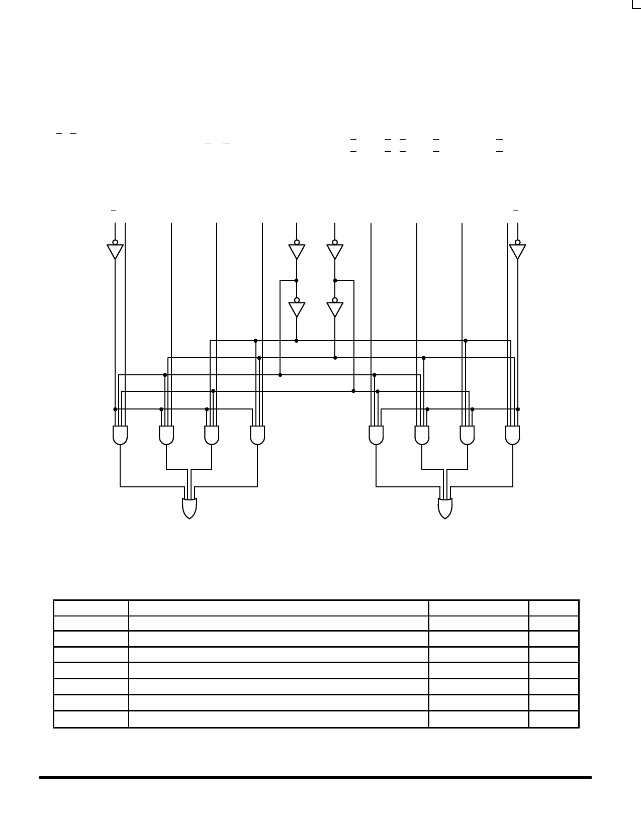
LOGIC DIAGRAM
Ea I0a
I1a
I2a
I3a
S1
S0
I0b
I1b
I2b
I3b Eb
Za
Zb
Please note that this diagram is provided only for the understanding of logic
operations and should not be used to estimate propagation delays.
MAXIMUM RATINGS*
Symbol
Parameter
Value
Unit
VCC
Vin
Vout
Iin
Iout
ICC
Tstg
DC Supply Voltage (Referenced to GND)
DC Input Voltage (Referenced to GND)
DC Output Voltage (Referenced to GND)
DC Input Current, per Pin
DC Output Sink/Source Current, per Pin
DC VCC or GND Current per Output Pin
Storage Temperature
–0.5 to +7.0
V
–0.5 to VCC +0.5
V
–0.5 to VCC +0.5
V
±20
mA
±50
mA
±50
mA
–65 to +150
°C
* Maximum Ratings are those values beyond which damage to the device may occur. Functional operation should be restricted to the Recommended
Operating Conditions.
FACT DATA
5-2
Share Link: 