FSA9280A Просмотр технического описания (PDF) - Fairchild Semiconductor
Номер в каталоге
Компоненты Описание
производитель
FSA9280A
Fairchild Semiconductor

FSA9280A Datasheet PDF : 30 Pages
| |||
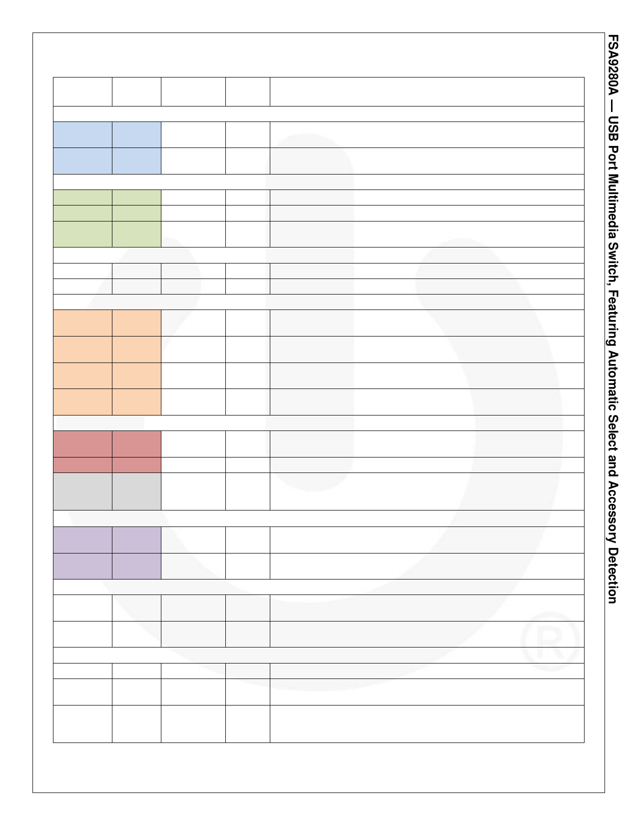
Pin Descriptions
Name
Pin #
USB Interface
DP_HOST
4
DM_HOST
5
Audio Interface
Audio_L
2
Audio_R
1
Type
Default
State
Description
Signal Path
Signal Path
Open
Open
D+ signal switch path, dedicated USB port to be connected to the resident
USB transceiver on the phone
D- signal switch path, dedicated USB port to be connected to the resident
USB transceiver on the phone
Signal Path
Signal Path
Open Left audio channel from mobile phone audio-out CODEC
Open Right audio channel from mobile phone audio-out CODEC
MIC
3
Signal Path Open Connected to the mobile phone audio CODEC MIC input pin
UART Interface
TxD
7
RxD
6
Connector Interface
ID_CON
20
Signal Path
Signal Path
Signal Path
DP_CON
19
Signal Path
DM_CON
18
Signal Path
VBUS_IN
17
Power Interface
Power Path
VBAT
11
Power
VDDIO
GND
9
Exposed
Center
Pad
Charger Interface
Power
Ground
VBUS_OUT
15
CHG_DET
16
Factory Interface
JIG
10
BOOT
8
I2C Interface
I2C_SCL
14
I2C_SDA
13
Power Path
Open-Drain
Output
Open-Drain
Output
CMOS
Output
Input
Open-Drain
I/O
INTB
12
CMOS
Output
Open Transmitter (Tx) from resident UART on the mobile phone
Open Receiver (Rx) from resident UART on the mobile phone
Open
Open
Open
N/A
Connected to the USB connector ID pin and used for detecting
accessories or button presses
Connected to the USB connector D+ pin; depending on the signaling
mode, this pin can be switched to DP_HOST, Audio_R, or RxD pins
Connected to the USB connector D- pin; depending on the signaling
mode, this pin can switched to DM_HOST, Audio_L, or TxD pins
Input voltage supply pin to be connected to the VBUS pin of the USB
connector
N/A
Input voltage supply pin to be connected to the mobile phone battery
output or to an internal regulator on the phone
N/A Baseband processor interface I/O supply pin
N/A Ground (center ground pad of package makes electrical contact)
N/A
Output voltage supply pin to be connected to the source voltage pin on
the charger IC
Hi-Z
Open-drain active LOW output, used to signal the charger IC that a
charger has been attached
Hi-Z
LOW
Output control signal driven by the FSA9280A and used by the processor
for factory test modes
Output control signal driven by the FSA9280A and used by the processor
for factory test modes
Hi-Z I2C serial clock signal to be connected to the phone-based I2C master
Hi-Z I2C serial data signal to be connected to the phone-based I2C master
LOW
Interrupt active LOW output used to prompt the phone baseband
processor to read the I2C register bits, indicates a change in ID_CON pin
status or accessory attach status
© 2009 Fairchild Semiconductor Corporation
FSA9280A • Rev 1.1.0
4
www.fairchildsemi.com
Share Link: