MT90737 Просмотр технического описания (PDF) - Mitel Networks
Номер в каталоге
Компоненты Описание
производитель
MT90737 Datasheet PDF : 40 Pages
| |||
CMOS MT90737
®
DS3/DS1 MUX/DEMUX (M13)
Preliminary Information
Features
• Multiplexes/demultiplexes 28 DS1 signals
to/from a DS3 signal
• Selectable M13 or C-bit parity mode
• Separate interface for C-bits
• FEBE, C or P-bit parity error insertion
• DS3 LOS, LOF, P-bit parity, C-bit parity, AIS
and idle signal detection
• DS3 AIS and idle signal generation
• Access to DS3 and DS2 X-bits
• DS3 and DS1 loopbacks
• Detects DS2 LOF
• DS1 idle signal (QRS, AIS or ESF) generation
• DS1 LOS detection on transmit or receive path
• Multiplexed and non-multiplexed
microprocessor bus interfaces
Applications
• Single-board M13 multiplexer
• Compact add/drop mux
• Fractional T3
• Digital Cross-connect Systems
• CSU/DSU
ISSUE 1
Ordering Information
June 1995
MT90737AM
208 Pin PQFP
-40° to 85°C
Description
The MT90737 DS3/DS1 Multiplexer/Demultiplexer
(M13) is designed to multiplex and demultiplex 28
independent DS1 signals to and from a DS3 signal
with either an M13 or C-bit frame format. The
MT90737 complies with Bellcore’s TR-TSY-000499,
ANSI’s T1.107-1988 and supplement T1.107a-1990.
The MT90737 provides a separate transmit (13 bits)
and receive (14 bits) interface for C-bits while
operating in the C-bit parity mode. The FEAC
channel (C3) is accessed via MT90737 memory. The
MT90737 uses 37 byte register locations for software
control, performance counters, and alarm reporting.
Both multiplexed and non-multiplexed bus types are
supported by the microprocessor interface.
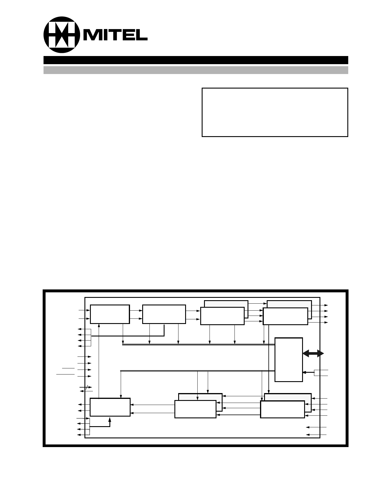
DS3DR
DS3CR
CDR
CCKR
CFMR
CDCCR
XCK
DLEN
TEST
OUTDIS
{ BOUNDARY
SCAN
DS3DT
DS3CT
CDT
CCKT
CFMT
CDCCT
DS3
Frame Sync
Loopback
4
DS3
Framing/Stuffing
U.S. Patent Number 5040170
DS3
Destuffing
7
1 DS2
Sync/Destuff
28
1
DS1
Outputs
Alarm/Status
Control
Loopback
Micro-
processor
I/O
Memory
Map
7
1 DS2
Framing/Stuffing
28
1
DS1
Input
Figure 1 - Functional Block Diagram
DR28
DR1
CR28
CR1
Micro-
processor
Interface
S7
S6
DT28
DT1
CT28
CT1
VSS
VDD
5-63
Share Link: 