L9949 Просмотр технического описания (PDF) - STMicroelectronics
Номер в каталоге
Компоненты Описание
производитель
L9949 Datasheet PDF : 20 Pages
| |||
L9949
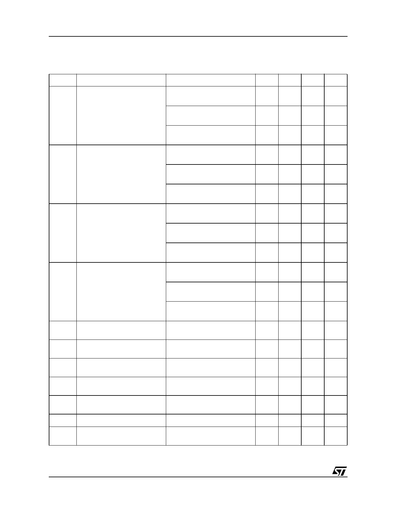
ELECTRICAL CHARACTERISTCS (continued)
VS = 8 to 16 V, VCC = 4.5 to 5.5 V, Tj = -40 to 150 °C, unless otherwise specified. The voltages are refered to
GND and currents are assumed positive, when the current flows into the pin.
Symbol
Parameter
Test Condition
Min. Typ. Max. Unit
RON OUT3 On-resistance to Supply or GND VS = 13.5 V, Tj = 25 °C,
IOUT3 = ± 0.8 A
800 mΩ
VS = 13.5 V, Tj = 125 °C,
IOUT3 = ± 0.8 A
1250 mΩ
VS = 8.0 V, Tj = 25 °C,
IOUT3 = ± 0.8 A
980 mΩ
RON OUT4 On-resistance to Supply or GND VS = 13.5 V, Tj = 25 °C,
IOUT4 = ± 0.8 A
800 mΩ
VS = 13.5 V, Tj = 125 °C,
IOUT4 = ± 0.8 A
1250 mΩ
VS = 8.0 V, Tj = 25 °C,
IOUT4 = ± 0.8 A
980 mΩ
RON OUT5 On-resistance to Supply or GND VS = 13.5 V, Tj = 25 °C,
IOUT5 = ± 0.8 A
800 mΩ
VS = 13.5 V, Tj = 125 °C,
IOUT5 = ± 0.8 A
1250 mΩ
VS = 8.0 V, Tj = 25 °C,
IOUT5 = ± 0.8 A
980 mΩ
RON OUT6 On-resistance to Supply
VS = 13.5 V, Tj = 25 °C,
IOUT6 = - 2.5 A
100 mΩ
VS = 13.5 V, Tj = 125 °C,
IOUT6 = - 2.5 A
150 mΩ
VS = 8.0 V, Tj = 25 °C,
IOUT6 = - 2.5 A
120 mΩ
|IOUT1| Output Current Limitation to
sink and source, current ramp
6
Supply or GND
10
A
|IOUT2| Output Current Limitation to
sink and source, current ramp
6
Supply or GND
10
A
|IOUT3| Output Current Limitation to
sink and source, current ramp
1.6
Supply or GND
2.5
A
|IOUT4| Output Current Limitation to
sink and source, current ramp
1.6
Supply or GND
2.5
A
|IOUT5| output current limitation to Supply sink and source, current ramp
1.6
or GND
2.5
A
|IOUT6| Output Current Limitation to GND source, current ramp
6.3
11
A
|IOUT6/res| Output Current Limitation to GND source, switching into resistive
5.1
switching into resistive load
load, go-nogo test
11
A
For details of the on-resistance (Ron over temperature) see the figures „Typical ron characteristics“ for the differential output stages
(FIGURE 3, FIGURE 4, FIGURE 5)
8/20
Share Link: 