X28C010D Просмотр технического описания (PDF) - Intersil
Номер в каталоге
Компоненты Описание
производитель
X28C010D Datasheet PDF : 23 Pages
| |||
X28C010
Page Write Operation
The page write feature of the X28C010 allows the entire
memory to be written in 5 seconds. Page write allows two to
two hundred fifty-six bytes of data to be consecutively written
to the X28C010 prior to the commencement of the internal
programming cycle. The host can fetch data from another
device within the system during a page write operation
(change the source address), but the page address (A8
through A16) for each subsequent valid write cycle to the part
during this operation must be the same as the initial page
address.
The page write mode can be initiated during any write
operation. Following the initial byte write cycle, the host can
write an additional one to two hundred fifty six bytes in the
same manner as the first byte was written. Each successive
byte load cycle, started by the WE HIGH to LOW transition,
must begin within 100µs of the falling edge of the preceding
WE. If a subsequent WE HIGH to LOW transition is not
detected within 100µs, the internal automatic programming
cycle will commence. There is no page write window
limitation. Effectively the page write window is infinitely wide,
so long as the host continues to access the device within the
byte load cycle time of 100µs.
Write Operation Status Bits
The X28C010 provides the user two write operation status
bits. These can be used to optimize a system write cycle
time. The status bits are mapped onto the I/O bus as shown
in Figure 1.
DATA Polling I/O7
Last
WE Write
I/O DP TB 5
4
3
2
1
0
Reserved
Toggle Bit
DATA Polling
FIGURE 1. STATUS BIT ASSIGNMENT
DATA Polling (I/O7)
The X28C010 features DATA Polling as a method to indicate
to the host system that the byte write or page write cycle has
completed. DATA Polling allows a simple bit test operation to
determine the status of the X28C010, eliminating additional
interrupt inputs or external hardware. During the internal
programming cycle, any attempt to read the last byte written
will produce the complement of that data on I/O7 (i.e., write
data = 0xxx xxxx, read data = 1xxx xxxx). Once the
programming cycle is complete, I/O7 will reflect true data.
Note: If the X28C010 is in the protected state, and an illegal
write operation is attempted, DATA Polling will not operate.
Toggle Bit (I/O6)
The X28C010 also provides another method for determining
when the internal write cycle is complete. During the internal
programming cycle, I/O6 will toggle from HIGH to LOW and
LOW to HIGH on subsequent attempts to read the device.
When the internal cycle is complete the toggling will cease
and the device will be accessible for additional read or write
operations.
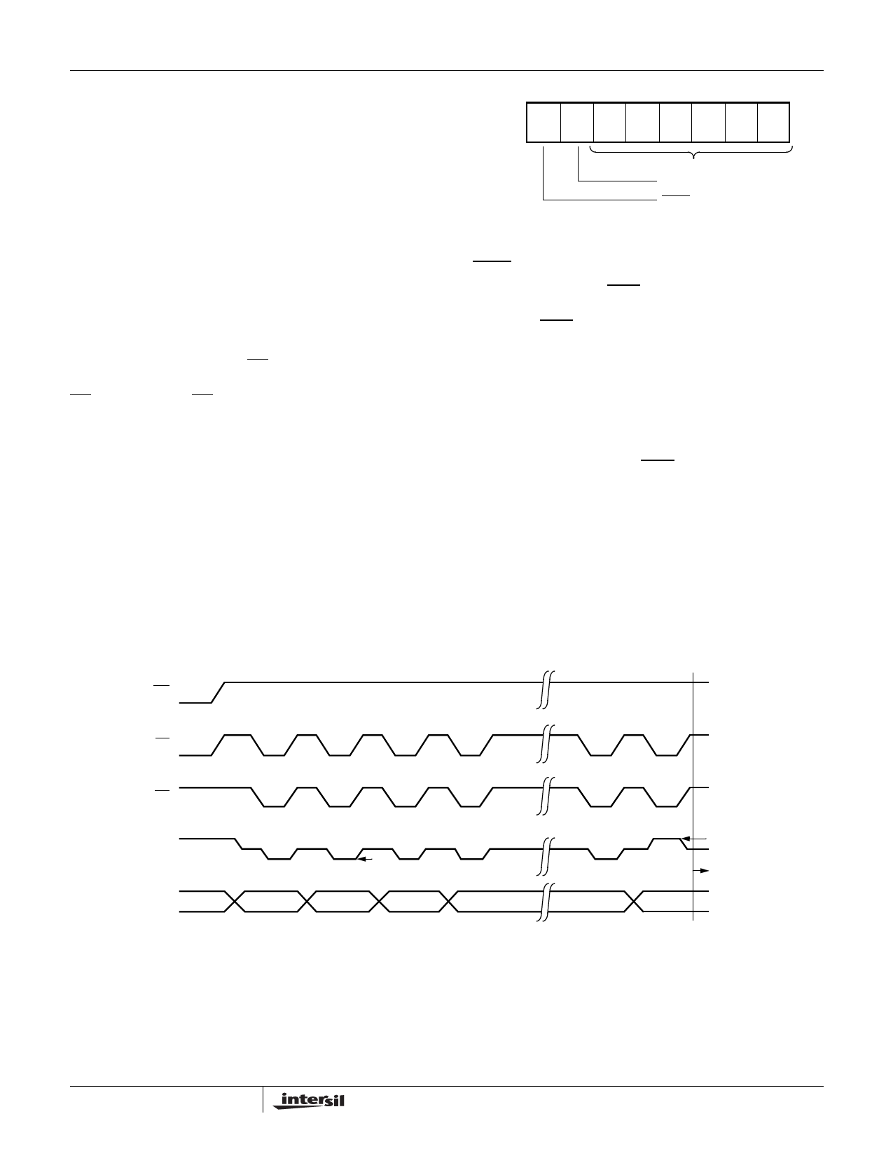
CE
OE
VIH
I/O7
A0-A14
An
HIGH Z
VOL
An
An
An
An
An
FIGURE 2. DATA POLLING BUS SEQUENCE
VOH
X28C010
Ready
An
4
FN8105.0
May 11, 2005
Share Link: 