X25043P-V Просмотр технического описания (PDF) - Xicor -> Intersil
Номер в каталоге
Компоненты Описание
производитель
X25043P-V Datasheet PDF : 15 Pages
| |||

X25043/45
The RESET (X25045) output is designed to go HIGH
whenever VCC has dropped below the minimum trip
point and/or the watchdog timer has reached its pro-
grammable time-out limit.
Operational Notes
The X25043/45 powers-up in the following state:
• The device is in the low power standby state.
• A HIGH to LOW transition on CS is required to
enter an active state and receive an instruction.
• SO pin is high impedance.
• The “write enable” latch is reset.
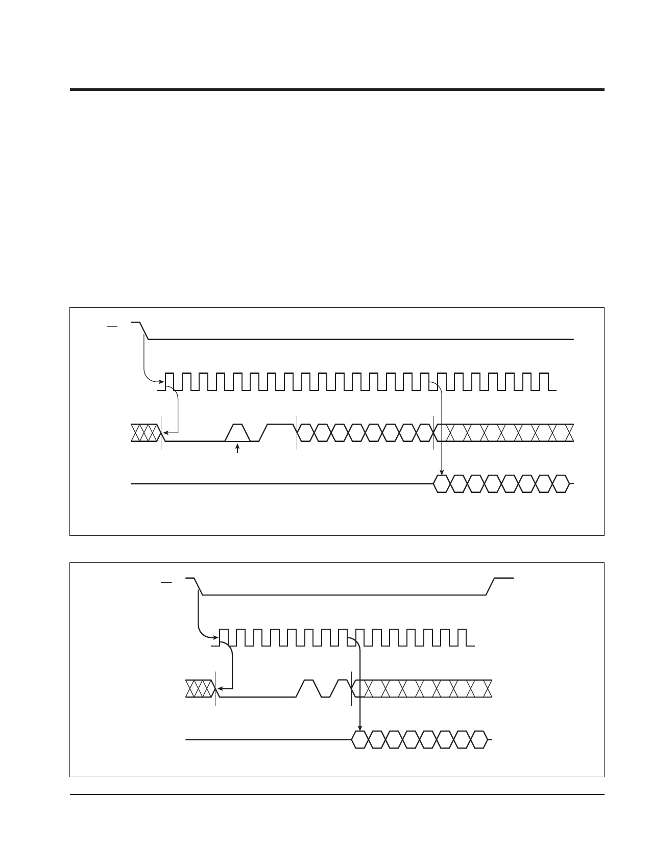
Figure 1. Read E2PROM Array Operation Sequence
Data Protection
The following circuitry has been included to prevent
inadvertent writes:
• The “write enable” latch is reset upon power-up.
• A WREN instruction must be issued to set the “write
enable” latch.
• CS must come HIGH at the proper clock count in
order to start a write cycle.
The “write enable” latch is reset when WP is brought
LOW.
CS
SCK
0 1 2 3 4 5 6 7 8 9 10 11 12 13 14 15 16 17 18 19 20 21 22
INSTRUCTION
BYTE ADDRESS
SI
8
76 5 4 3 2 1 0
9TH BIT OF ADDRESS
HIGH IMPEDANCE
SO
DATA OUT
76543210
MSB
3844 FHD F04
Figure 2. Read Status Register Operation Sequence
CS
SCK
0 1 2 3 4 5 6 7 8 9 10 11 12 13 14
INSTRUCTION
SI
HIGH IMPEDANCE
SO
DATA OUT
76543210
MSB
3844 ILL F15
5