WED3C7410E16M400BC Просмотр технического описания (PDF) - White Electronic Designs Corporation
Номер в каталоге
Компоненты Описание
производитель
WED3C7410E16M400BC Datasheet PDF : 13 Pages
| |||
White Electronic Designs WED3C7410E16M-XBX
POWER CONSUMPTION
VCC = AVCC = 1.8 ±0.1V VDC, L2VCC = 3.3V ±5% VDC, GND = 0 VDC, 0 ≤ TJ < 105°C
Processor (CPU) Frequency/L2 Frequency
Full-on Mode
Doze Mode
Nap Mode
Sleep Mode
Sleep Mode–PLL and DLL Disabled
Typical
Maximum
Maximum
Maximum
Maximum
Maximum
400MHz/200MHz
450MHz/200MHz
Unit
5.7
6.2
W
13.1
14.3
W
5.3
5.8
W
2.25
2.4
W
2.20
2.35
W
2.0
2.0
W
Notes
1, 3
1, 2
1, 2
1, 2
1, 2
1, 2
NOTES:
1. These values apply for all valid system bus and L2 bus ratios. The values do not include OVCC; AVCC and L2AVCC suppling power. OVCC power is system dependent, but is typically
<10% of VCC power. Worst case power consumption, for AVCC = 15mW and L2AVCC = 15mW.
2. Maximum power is measured at VCC = 1.9 V while running an entirely cache-resident, contrived sequence of instructions which keep the execution units maximally busy.
3. Typical power is an average value measured at VCC = AVCC = L2AVCC = 1.8V, OVCCd = L2OVCC = 2.5V in a system, executing typical applications and benchmark sequences.
4. At a maximum 60x bus frequency of 133MHz, the maximum configurtable core frequency is 400MHz.
BGA THERMAL RESISTANCE
Description
Symbol
PPC
SSRAM
Junction to Ambient (No Airflow)
Theta JA
14.0
10.3
Junction to Ball
Theta JB
8.9
5.2
Junction to Case (Top)
Theta JC
0.1
0.1
NOTE 1: Refer to PBGA Thermal Resistance Correlation at www.whiteedc.com in the application notes section for modeling conditions
Units
C/W
C/W
C/W
Notes
1
1
1
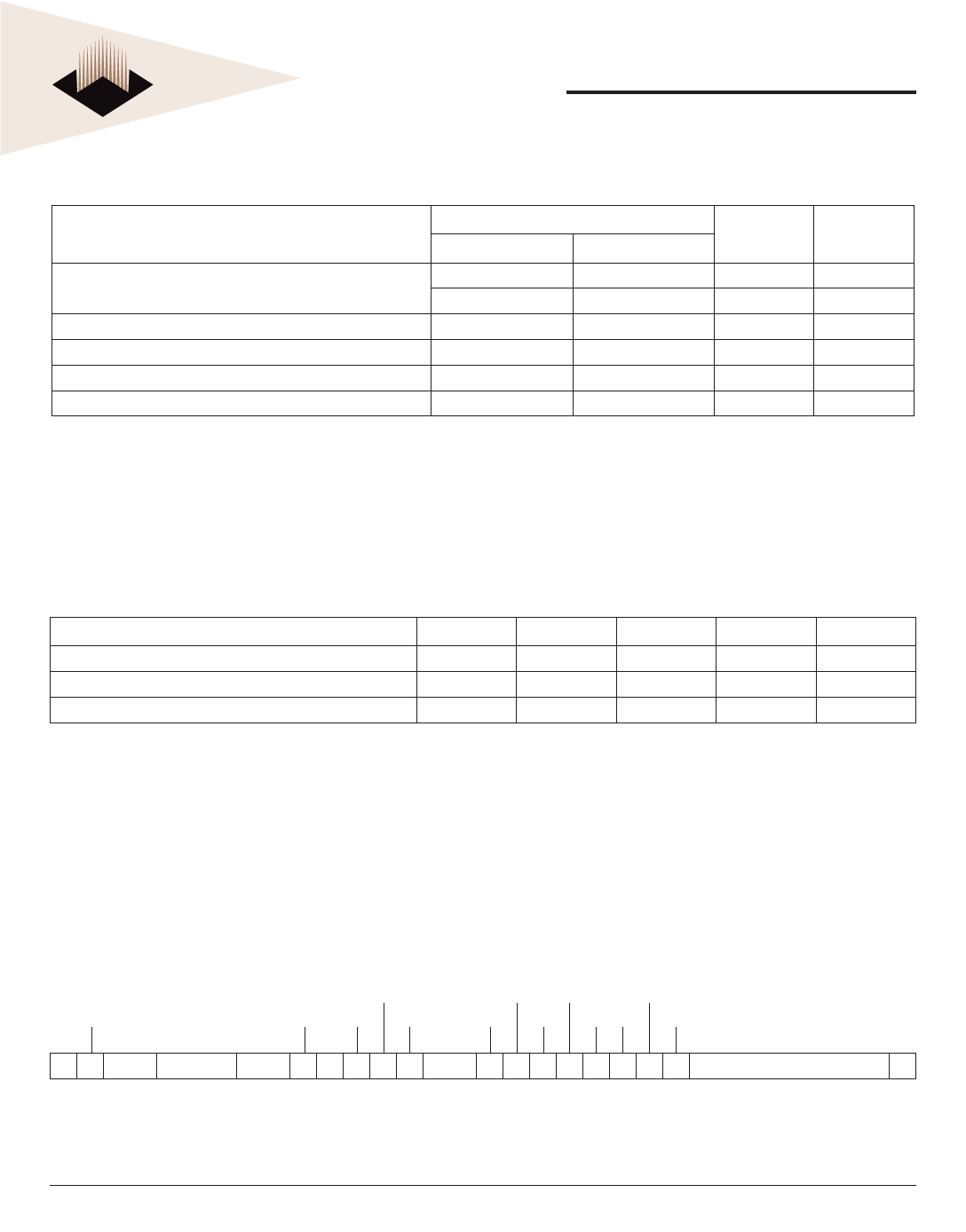
L2 CACHE CONTROL REGISTER (L2CR)
The L2 cache control register, shown in Figure 5, is a supervisor-level, implementation-specific SPR used to configure
and operate the L2 cache. It is cleared by hard reset or power-on reset.
FIGURE 5 – L2 CACHE CONTROL REGISTER (L2CR)
L2WT
L2DF L2FA L2CLKSTP
L2PE
L2DO L2CTL L2TS
L2SL L2BYP L2HWF L2IO L2DRO
L2IP
L2E
L2SIZ L2CLK L2RAM L21
L2OH
0 1 2 34
6 7 8 9 10 11 12 13 14 15 16 17 18 19 20 21 22 22 24
The L2CR bits are described in Table 1.
0000000
30 31
May 2006
Rev. 9
8
White Electronic Designs Corporation • (602) 437-1520 • www.wedc.com
Share Link: 