VSC8169 Просмотр технического описания (PDF) - Vitesse Semiconductor
Номер в каталоге
Компоненты Описание
производитель
VSC8169 Datasheet PDF : 18 Pages
| |||
VITESSE
SEMICONDUCTOR CORPORATION
OC-48 (FEC) 16:1 SONET/SDH
MUX with Clock Generator
Preliminary Data Sheet
VSC8169
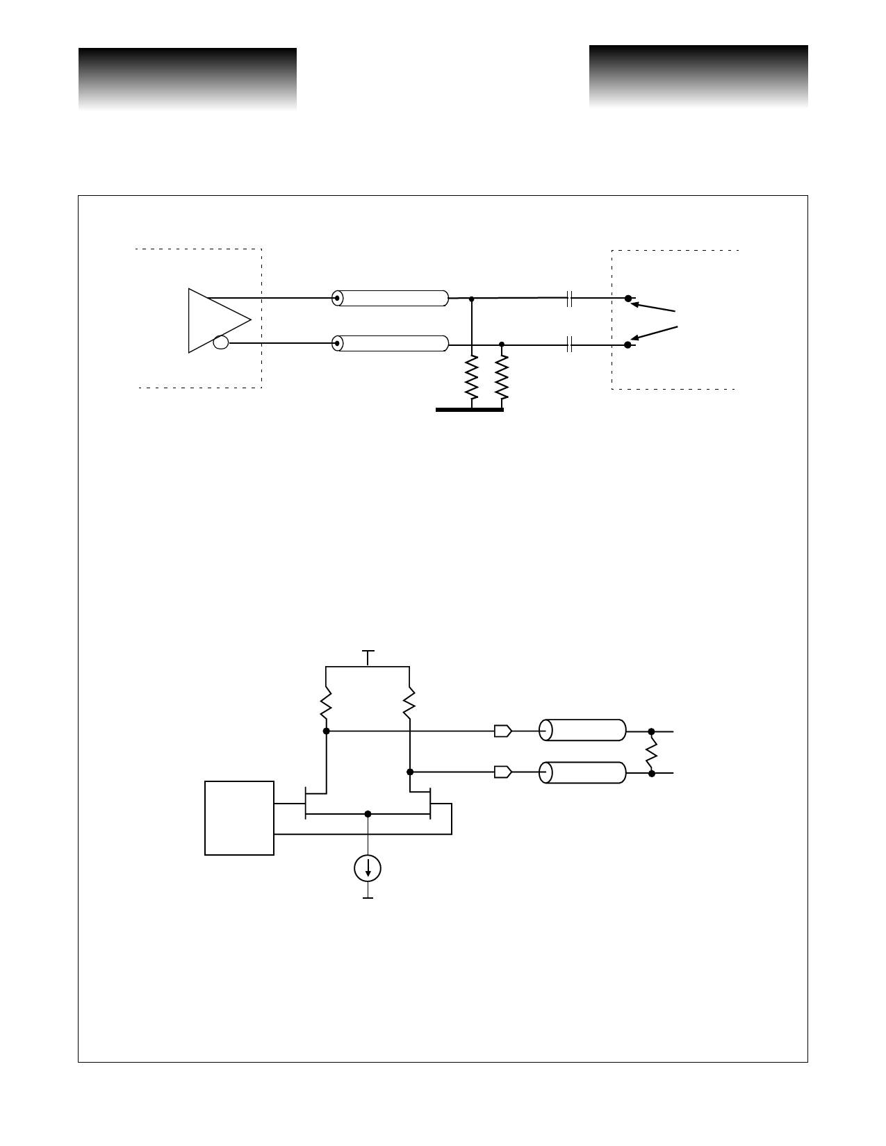
Figure 5: AC Termination of CLK16O+/-, REFCLKO+/-
VSC8169
Zo
Zo
50Ω
100nF
50Ω 100nF
VCC-2V
downstream
bias point
generated
internally
High-Speed Data and Clock Output
The high-speed data and clock output drivers consist of a differential pair designed to drive a 50Ω transmis-
sion line. The transmission line should be terminated with a 100Ω resistor at the load between true and comple-
ment outputs (see Figure 6). Connection to a termination voltage is not required. The output driver is back
terminated to 50Ω on-chip, providing a snubbing of any reflections. If used single-ended, the high-speed output
driver must still be terminated differentially at the load with a 100Ω resistor between true and complement out-
puts. The high-speed clock output can be powered down for additional power savings. To power down the high-
speed clock, tie the associated pins to VCC (see Table 3, Package Pin Identifications, pins 5,6,7).
Figure 6: High-Speed Output Termination
VCC
50Ω
Pre-Driver
50Ω
100Ω
Z0 = 50Ω
VEE
Clock Generator
An on-chip PLL generates the 2.48832GHz (or up to 2.7GHz for FEC) transmit clock from the externally
provided REFCLK input. The on-chip PLL uses a low phase noise reactance-based Voltage Controlled Oscilla-
tor (VCO) with an on-chip loop filter. The loop bandwidth of the PLL is within the SONET specified limit of
2MHz.
Page 4
© VITESSE SEMICONDUCTOR CORPORATION • 741 Calle Plano • Camarillo, CA 93012
Tel: (800) VITESSE • FAX: (805) 987-5896 • Email: prodinfo@vitesse.com
Internet: www.vitesse.com
G52230-0, Rev 3.6
01/02/01
Share Link: 