VRE4100 Просмотр технического описания (PDF) - Cirrus Logic
Номер в каталоге
Компоненты Описание
производитель
VRE4100 Datasheet PDF : 8 Pages
| |||
Product Innova tionFrom
VRE4100
Reverse Current Path
The P-channel pass transistor used in this series has an inherent diode connected between the Vin and VOUT pins.
Forcing the output to voltages higher than the input or pulling Vin below the voltage stored in the output capacitor
by more than the Vbe will forward bias this diode and current will flow from the Vout pin to Vin. This will not damage
the device as long as the current does not exceed 50 mA.
ON/OFF Operation
This series features a sleep mode that is activated by pulling the enable pin low. To turn the reference on, the en-
able pin is pulled high. If this feature is not used, the enable pin should be tied to Vin to keep the reference on at all
times. The enable pin must not be left unconnected (floating).
When powered off, these devices will quickly reduce both Vout and IQ to zero. During power down, the charge
across the output capacitor is discharged to ground through the internal circuitry. On power up, the Vout is restored
in less than 200 μs.
The signal source used to drive the enable pin can come from either a totem-pole output or an open collector output
with a pull-up resistor to the input voltage. The signal source must be able to swing above and below the voltage
thresholds to guarantee an ON or OFF state. It must not exceed the absolute maximum rating for the enable pin.
Output Accuracy
The output accuracy after assembly at room temperature is made up of three components: initial accuracy of the de-
vice, thermal hysteresis, and mechanical stress. The initial accuracy is measured at the factory and may not reflect
the actual output voltage when the devices are mounted to a PCB. The effects of mechanical stress and thermal
hysteresis can shift the output voltage.
Thermal Hysteresis
Thermal hysteresis is a change in output voltage as a result of a temperature change. When references experience
a temperature change and return to the initial temperature, they do not always have the same initial voltage. Ther-
mal hysteresis is difficult to correct and is a major error source in systems that experience temperature changes
greater than 25°C. Reference vendors are starting to include this important specification in their datasheets
Mechanical Hysteresis
Recommendations to minimize mechanical stress:
1) Mount the VRE4112/VRE4125/VRE4141 near the edges or corners of the PCB. The center of the board generally
has the highest mechanical and thermal stress.
2) Mechanically isolate the device by cutting a U shaped slot around the package. This provides some mechanical
and thermal isolation from the rest of the circuit.
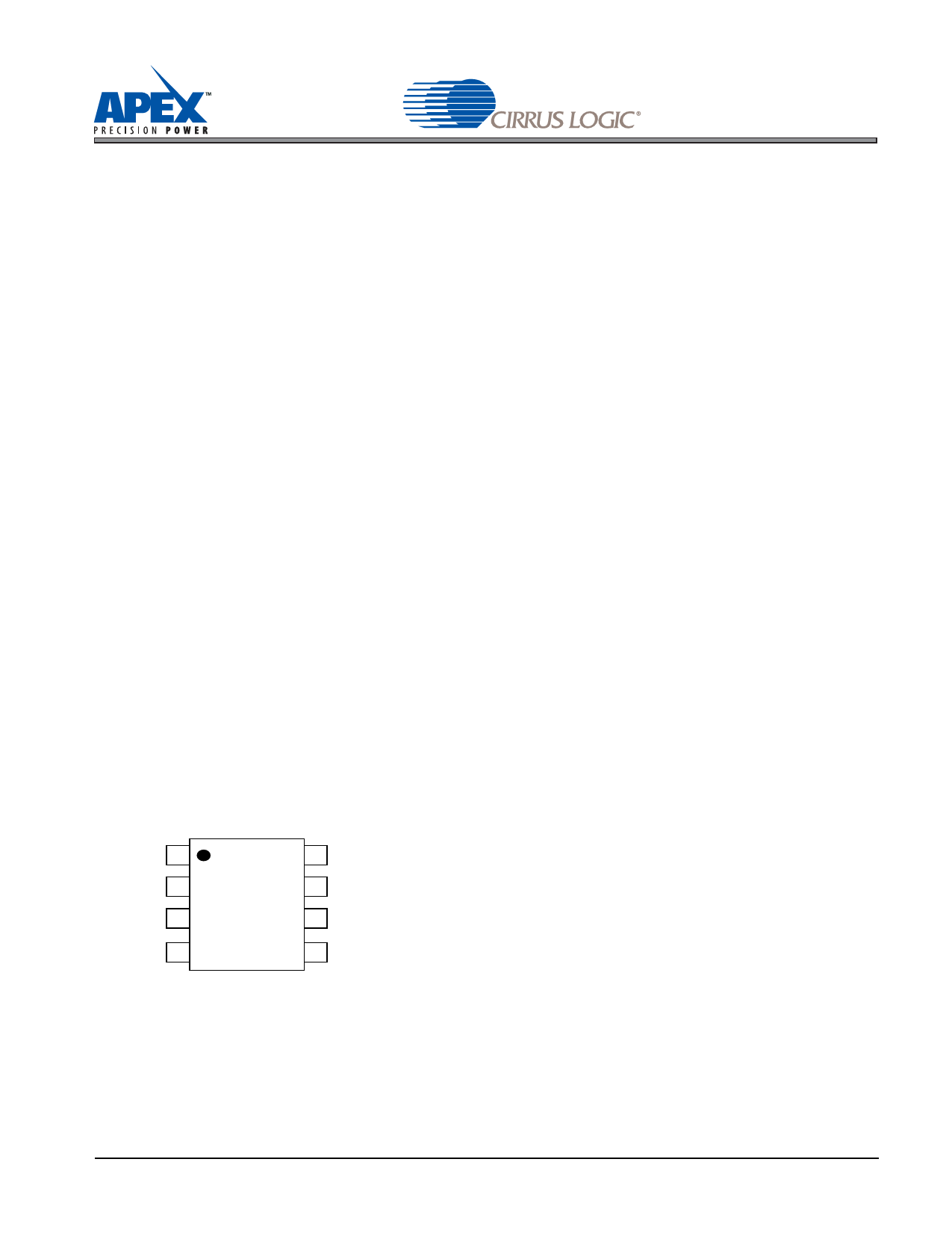
PIN CONFIGURATION
NC 1
+VIN 2
Enable 3
GND 4
VRE4100
TOP
VIEW
8 NC
7 NC
6 VREF
5 NC
VRE4100DS
Share Link: 