VRE4100 Просмотр технического описания (PDF) - Cirrus Logic
Номер в каталоге
Компоненты Описание
производитель
VRE4100 Datasheet PDF : 8 Pages
| |||
VRE4100
Product Innova tionFrom
1. Characteristics and Specifications
ABSOLUTE MAXIMUM RATINGS
Power Supply to any input pin.......-0.3V to +5.6V
Operating Temp. (B,C)...................... 0ºC to 70ºC
Operating Temp. (K).....................-40ºC to +85ºC
Storage Temperature Range......-65ºC to +150ºC
Output Short Circuit Duration............................... Indefinite
ESD Susceptibility Human Body Model....................... 2kV
ESD Susceptibility Machine Model............................ 200V
Lead Temperature (soldering, 10 sec)....................+260ºC
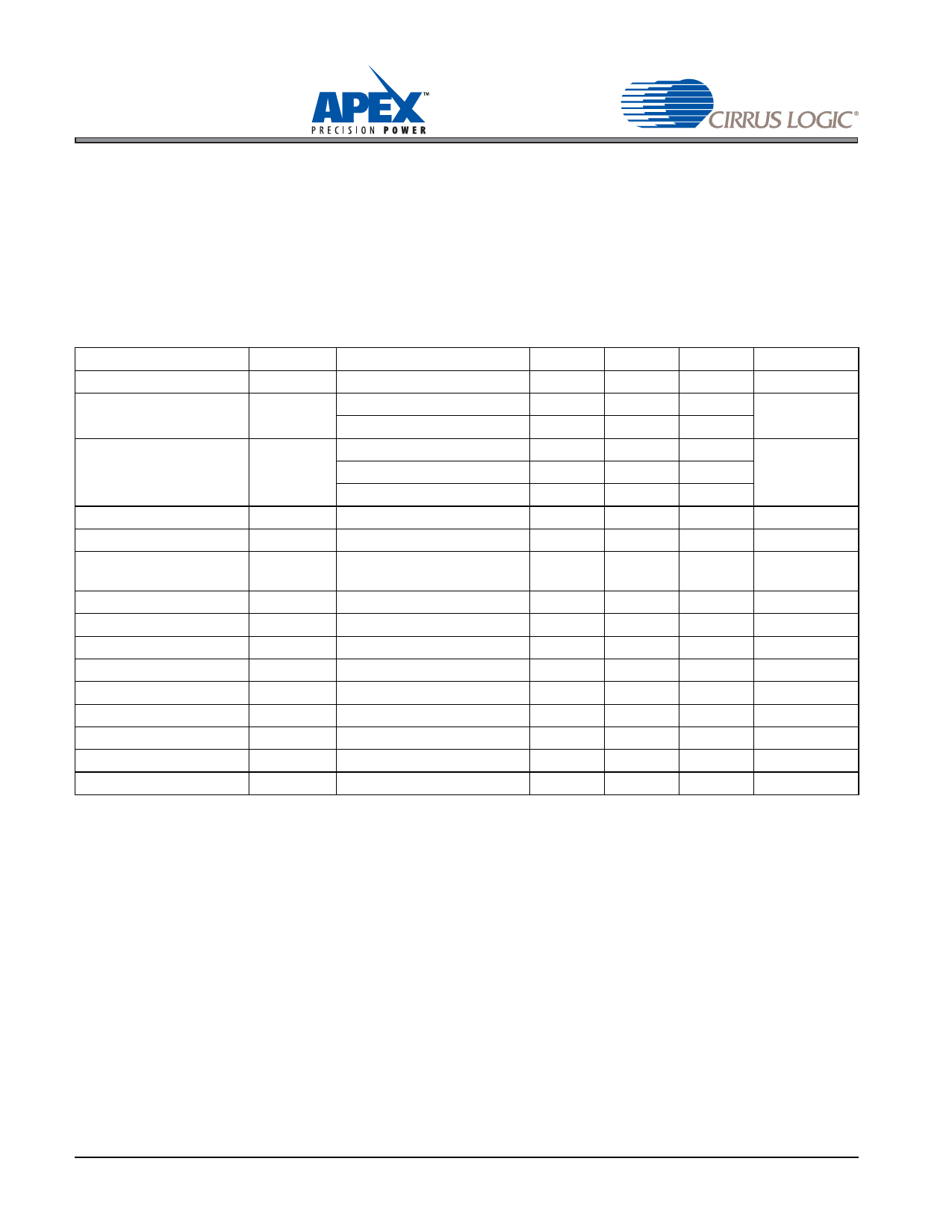
ELECTRICAL Specifications
VPS = +3 V for VRE4112, VPS = +5 V for VRE4125 and VRE4141. T = +25ºC, ILOAD = 1mA, COUT = 1µF Unless Otherwise Noted.
Parameter
Input Voltage
Output Voltage Error
(Note 1)
Output Voltage
Temperature Coefficient
(Note 2)
Symbol
VIN
VOUT
TCVOUT
Conditions
B Grade
C/K Grade
B Grade
C Grade
K Grade
Min
Typ
Max
+1.8
+5.5
±0.025 ±0.050
±0.040 ±0.080
+0.5
+1.0
+1.0
+2.0
+1.5
+3.0
Units
V
%
ppm/ºC
Dropout Voltage (Note 3)
Turn-On Settling Time
Output Noise Voltage
(Note 4)
Temperature Hysteresis
VIN - VOUT
TON
En
IL = 8mA
To 0.01% of final value
0.1Hz < f < 10Hz
Note 5
160
235
2
2.2
20
mV
µs
µVp-p
ppm
Long Term Stability
∆VOUT/T
1000 Hours
50
ppm
Supply Current
IIN
VLOAD = 0mA
230
320
µA
Load Regulation (Note 6) ∆VOUT/ ∆IOUT
1mA ≤ ILOAD ≤ 8mA
1
20
ppm/mA
Line Regulation (Note 6) ∆VOUT/ ∆VIN VREF + 200mV ≤ VIN ≤ 5.5V
20
200
ppm/V
Logic High Input Voltage
VH
0.8
V
Logic High Input Current
IH
2
nA
Logic Low Input Voltage
VL
0.4
V
Logic Low Input Current
IL
1
nA
NOTES:
1. High temperature and mechanical stress can effect the initial accuracy of this reference series.See
discussion on output accuracy.
2. The temperature coefficient is determined by the box method. See discussion on temperature perfor-
mance. All units are 100% tested over temperature.
3. The minimum input to output differential voltage at which the output voltage drops by 0.5% from
nominal.
4. Based on 1.024 V output. Noise is linearly proportional to VREF.
5. Defined as change in 25ºC output voltage after cycling device over operating temperature range.
6. Line and load regulation are measured with pulses and do not include output voltage changes due to
self heating.
VRE4100DS
Share Link: 