VRE3025 Просмотр технического описания (PDF) - Cirrus Logic
Номер в каталоге
Компоненты Описание
производитель
VRE3025 Datasheet PDF : 7 Pages
| |||
VRE3025
Product Innova tionFrom
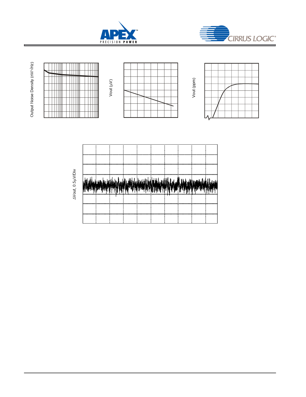
OUTPUT NOISE-VOLTAGE
DENSITY vs. FREQUENCY
50
40
30
20
10
10
100
1k
10k
Frequency (Hz)
CHANGE IN OUTPUT VOLTAGE
VS. OUTPUT CURRENT
400
300
200
100
0
-100
-200
-300
-400
0 2 4 6 8 10 12 14 16
Iout(mA)
0.1Hz to 10Hz Noise
CHANGE IN OUTPUT VOLTAGE
VS. INPUT VOLTAGE
60
50
40
30
20
10
0
-10
-20
0
9 10 11 12 13 14 15 16
Vin(V)
1 Sec/Div
3. THEORY OF OPERATION
The following discussion refers to the block diagram in Figure 1. A FET current source is used to bias a 6.3 V zener
diode. The zener voltage is divided by the resistor network R1 and R2. This voltage is then applied to the noninvert-
ing input of the operational amplifier which amplifies the voltage to produce a 2.5 V output. The gain is determined
by the resistor networks R3 and R4: G=1 + R4/R3. The 6.3 V zener diode is used because it is the most stable
diode over time and temperature.
The current source provides a closely regulated zener current, which determines the slope of the references’ volt-
age vs. temperature function. By trimming the zener current a lower drift over temperature can be achieved. But
since the voltage vs. temperature function is nonlinear this compensation technique is not well suited for wide tem-
perature ranges.
A nonlinear compensation network of thermistors and resistors that is used in the VRE series voltage references.
This proprietary network eliminates most of the nonlinearity in the voltage vs. temperature function. By adjusting the
slope, a very stable voltage is produced over wide temperature ranges.
This network is less than 2% of the overall network resistance so it has a negligible effect on long term stability. The
proper connection of the VRE3025 series voltage references with the optional trim resistor for initial error and the
optional capacitor for noise reduction is shown below.
4
VRE3025DS
Share Link: 