VN16118 Просмотр технического описания (PDF) - Vaishali Semiconductor
Номер в каталоге
Компоненты Описание
производитель
VN16118 Datasheet PDF : 10 Pages
| |||
VN16118
Table 6. Transceiver Reference Clock Requirements
TA = 0°C to +70°C, VCC = 3.15 V to 3.45 V
Symbol
Parameter
f
Nominal Frequency (for gigabit Ethernet
Compliance)
F tol
Symm
Frequency Tolerance
Symmetry (Duty Cycle)
Preliminary
Min. Typ. Max. Unit
125
MHz
-100
40
+100 ppm
60 %
Table 7. Transmitter Timing Characteristics
TA = 0°C to +70°C, VCC = 3.15 V to 3.45 V
Symbol
Parameter
t setup
Setup Time to Rising Edge of REFCLK
t hold
t_txlat [1]
Hold Time to Rising Edge of REFCLK
Transmitter Latency
Min.
1.5
1.0
Typ.
3.5
Max.
Unit
nsec
nsec
nsec
4.4
bits
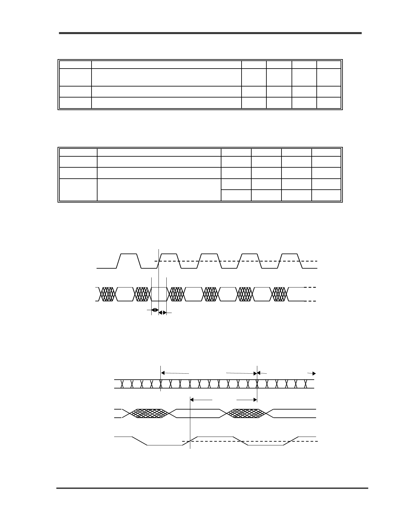
Note:
1. The transmitter latency, as shown in Figure 4, is defined as the time between the latching in of the
parallel data word (as triggered by the rising edge of the transmit by clock, REFCLK) and the
transmission of the first serial bit of that parallel word (defined by the rising edge of the first bit
transmitted).
TX_CLK
TX<9:0>
1.4 V
DATA
DATA
DATA
tSETUP
tHOLD
DATA
DATA
DATA
2.0 V
0.8 V
Figure 3. Transmitter Section
Timing
DATA BYTE A
DATA BYTE B
DOUT± T5 T6 T7 T8 T9 T0 T1 T2 T3 T4 T5 T6 T7 T8 T9 T0 T1 T2 T3 T4 T5
TX<9:0>
t_TXLAT
DATA BYTE B
DATA BYTE C
TX_CLK
1.4 V
Figure 4. Transmitter Latency
1999-12-15
Page 8
MDSN-0001-00
Vaishali Semiconductor l 747 Camden Avenue l Campbell l CA 95008 l Ph. 408.379.2900 l Fax 408.379.2937
Share Link: 