VN16BSP13TR Просмотр технического описания (PDF) - STMicroelectronics
Номер в каталоге
Компоненты Описание
производитель
VN16BSP13TR Datasheet PDF : 11 Pages
| |||
VN16BSP
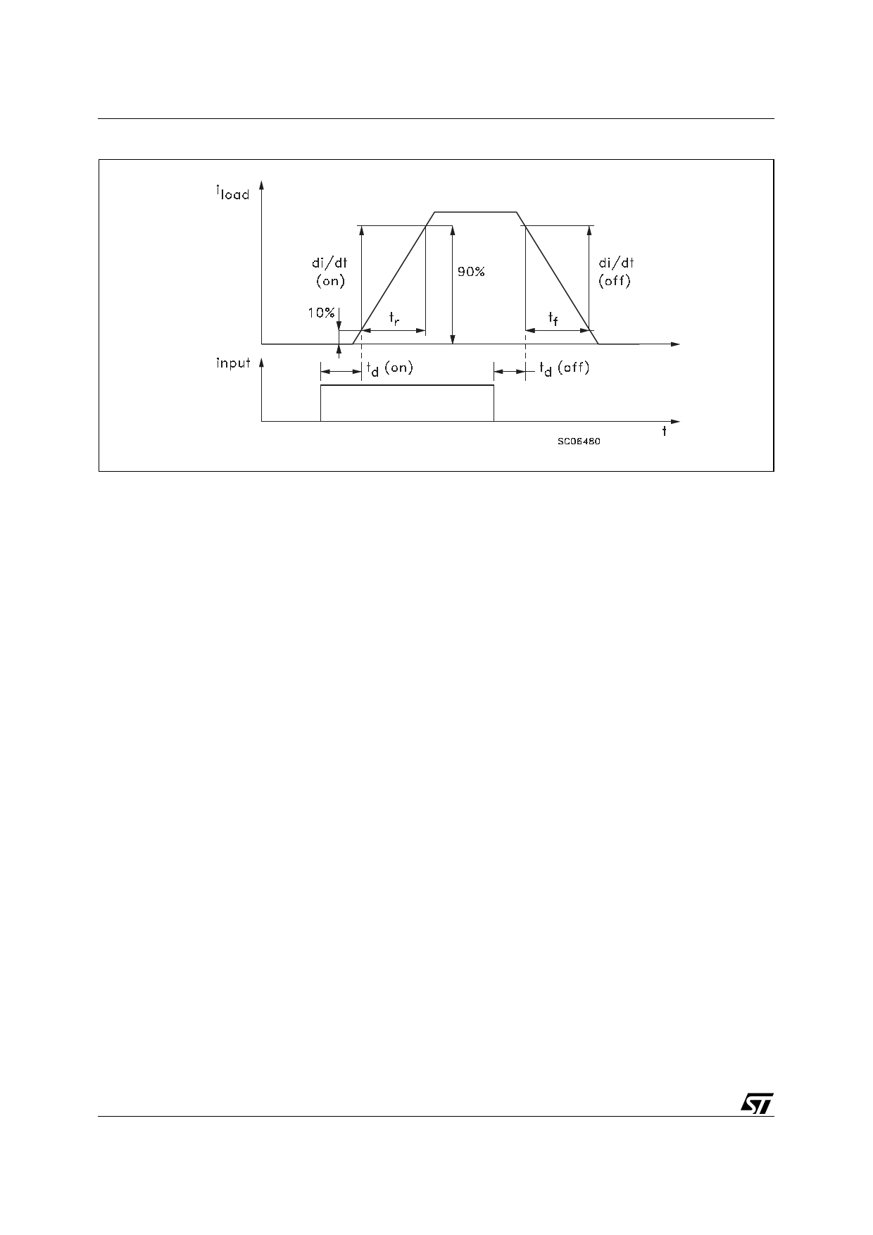
Figure 7. Switching Time Waveforms
FUNCTIONAL DESCRIPTION
The device has a diagnostic output which
indicates open load in on-state, open load in off-
state, over temperature conditions and stuck-on to
VCC.
From the falling edge of the input signal, the status
output, initially low to signal a fault condition
(overtemperature or open load on-state), will go
back to a high state with a different delay in case
of overtemperature (tpovl) and in case of open
load (tpol) respectively. This feature allows to
discriminate the nature of the detected fault. To
protect the device against short circuit and over
current condition, the thermal protection turns the
integrated Power MOS off at a minimum junction
temperature of 140 °C. When this temperature
returns to 125°C the switch is automatically turned
on again. In short circuit the protection reacts with
virtually no delay, the sensor being located inside
the Power MOS area. An internal function of the
devices ensures the fast demagnetization of
inductive loads with a typical voltage (Vdemag) of -
18V. This function allows to greatly reduces the
power dissipation according to the formula:
Pdem = 0.5 • Lload • (Iload)2 • [(VCC+Vdemag)/
Vdemag] • f
where f = switching frequency and
Vdemag = demagnetization voltage
The maximum inductance which causes the chip
temperature to reach the shut-down temperature
in a specified thermal environment is a function of
the load current for a fixed VCC, Vdemag and f
according to the above formula. In this device if the
GND pin is disconnected, with VCC not exceeding
16V, it will switch off.
PROTECTING THE DEVICE AGAINST
REVERSE BATTERY
The simplest way to protect the device against a
continuous reverse battery voltage (-26V) is to
insert a Schottky diode between pin 1 (GND) and
ground, as shown in the typical application circuit
(Figure 10).
The consequences of the voltage drop across this
diode are as follows:
– If the input is pulled to power GND, a negative
voltage of -Vf is seen by the device. (VIL, VIH
thresholds and VSTAT are increased by Vf with
respect to power GND).
– The undervoltage shutdown level is increa- sed
by Vf.
If there is no need for the control unit to handle
external analog signals referred to the power
GND, the best approach is to connect the
reference potential of the control unit to node [1]
(see application circuit in Figure 10), which
becomes the common signal GND for the whole
control board avoiding shift of VIH, VIL and VSTAT.
This solution allows the use of a standard diode.
6/11
Share Link: 