VN16BSP Просмотр технического описания (PDF) - STMicroelectronics
Номер в каталоге
Компоненты Описание
производитель
VN16BSP Datasheet PDF : 11 Pages
| |||
VN16BSP
ELECTRICAL CHARACTERISTICS
(8 < VCC < 16 V; -40 ≤ Tj ≤ 125 °C unless otherwise specified)
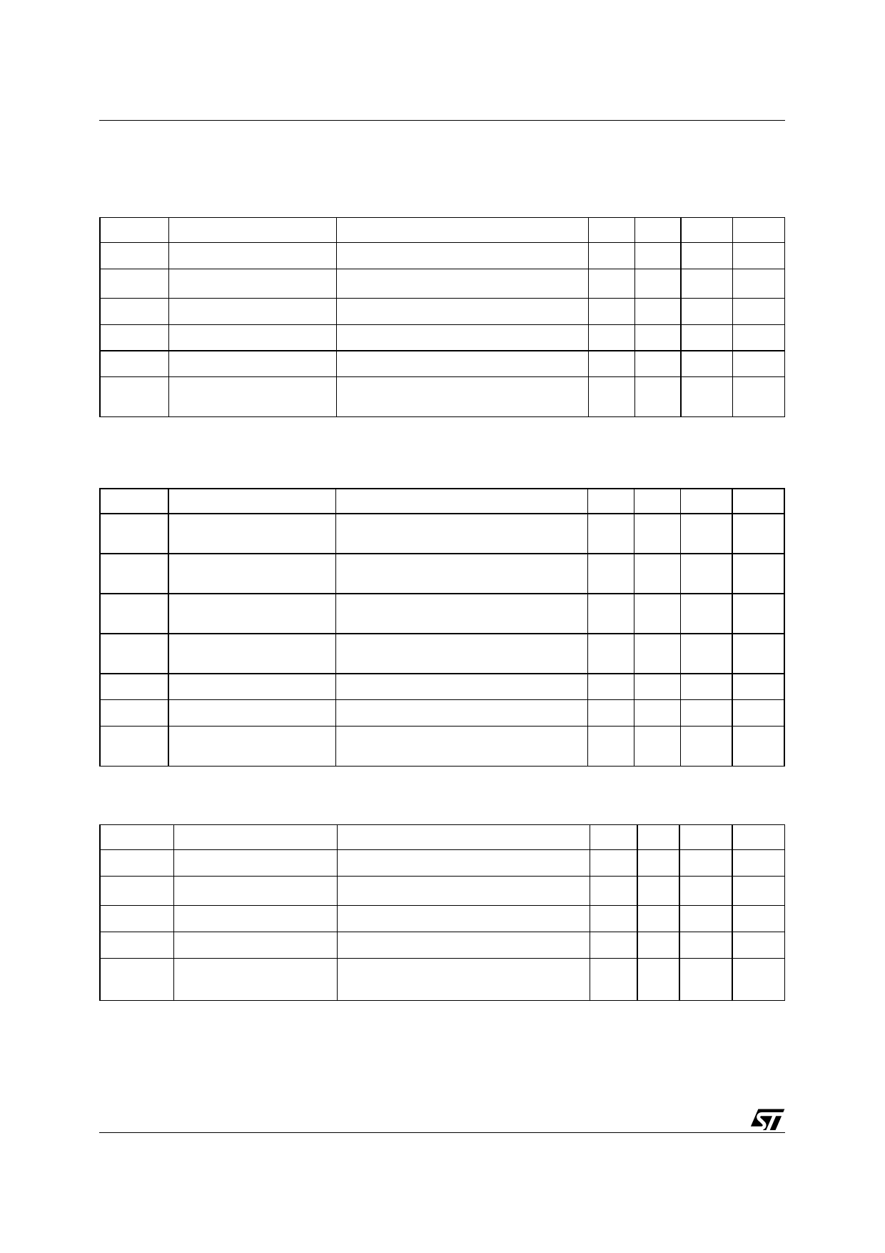
Table 5. Power
Symbol
Parameter
Test Conditions
Min. Typ. Max. Unit
VCC Supply Voltage
6
13
26
V
In(2)
Nominal Current
Tc = 85 °C; VDS(on) ≤ 0.5; VCC = 13 V
5.6
8.8
A
Ron On State Resistance
IOUT = In; VCC = 13 V; Tj = 25 °C
0.038
0.06
Ω
IS
Supply Current
Off State; VCC = 13 V; Tj ≥ 25 °C
25
50
µA
VDS(MAX) Maximum Voltage Drop
IOUT = 20 A; VCC = 13 V; Tc = 85 °C
1
1.8
V
Rj
Output to GND Internal
Tj = 25 °C
Impedance
5
10
20
KΩ
Note: 2. In= Nominal current according to ISO definition for high side automotive switch. The Nominal Current is the current at Tc = 85 °C
for battery voltage of 13V which produces a voltage drop of 0.5 V.
Table 6. Switching
Symbol
Parameter
td(on)(3) Turn-on Delay Time Of
Output Current
tr(3)
Rise Time Of Output
Current
td(off)(3) Turn-off Delay Time Of
Output Current
tf(3)
Fall Time Of Output
Current
(di/dt)on Turn-on Current Slope
(di/dt)off Turn-off Current Slope
Vdemag Inductive Load Clamp
Voltage
Note: 3. See Switching Time Waveforms.
Test Conditions
Rload = 1.6 Ω
Rload = 1.6 Ω
Rload = 1.6 Ω
Rload = 1.6 Ω
Rload = 1.6 Ω; VCC = 13 V
Rload = 1.6 Ω; VCC = 13 V
Rload = 1.6 Ω; L = 1 mH
Min. Typ. Max. Unit
5
50 500
µs
40 100 680
µs
10 100 500
µs
40 100 680
µs
0.008
0.1 A/µs
0.008
0.1 A/µs
–24 –18 –14
V
Table 7. Logic Input
Symbol
Parameter
Test Conditions
Min. Typ. Max. Unit
VIL
Input Low Level Voltage
1.5
V
VIH
Input High Level Voltage
3.5
Note 4 V
VI(hyst) Input Hysteresis Voltage
0.2
1
1.5
V
IIN
Input Current
VIN = 5 V; Tj = 25 °C
100
µA
VICL Input Clamp Voltage
IIN = 10 mA
IIN = –10 mA
5
6
7
V
–0.7
V
Note: 4. The VIH is internally clamped at 6V about. It is possible to connect this pin to an higher voltage via an external resistor calculated
to not exceed 10 mA at the input pin.
4/11
Share Link: 