HSP50016-EV Просмотр технического описания (PDF) - Intersil
Номер в каталоге
Компоненты Описание
производитель
HSP50016-EV Datasheet PDF : 18 Pages
| |||
HSP50016-EV
COMMAND
WCW
RCW
WCS
RCS
DIN
CLK
RES
IQS
RDO
PDF
ODF
TCK
TRS
TMS
TDI
TDO
PTF
PP
PPC
ERR
?
BYE, EXIT,
QUIT
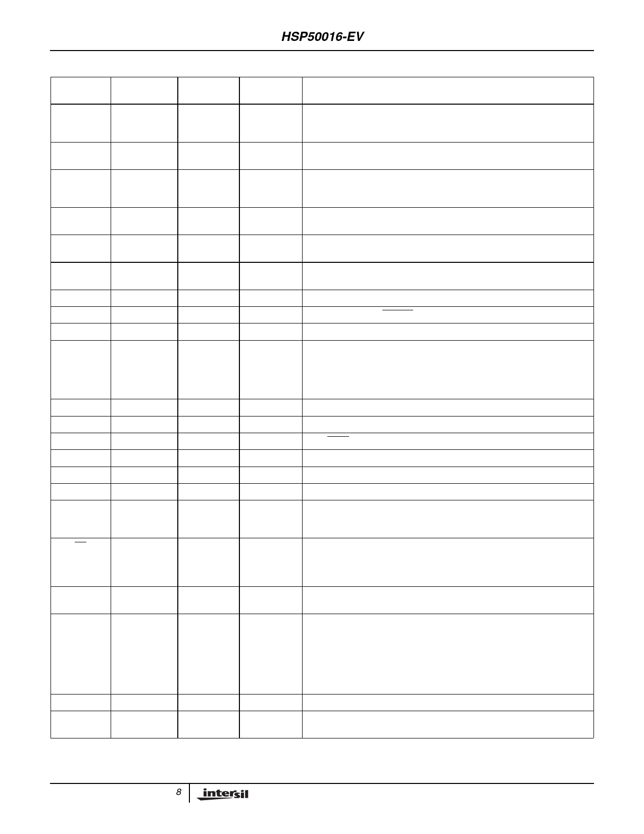
TABLE 2. COMMAND LIST FOR COMMAND LINE INTERFACE SOFTWARE
ARGUMENT ARGUMENT ARGUMENT
#1
#2
#3
COMMAND DESCRIPTION
WORD
NUMBER
UPDATE
BIT
CONTROL
WORD
Loads the specified control word of the HSP50016 with the 36-bit hexadeci-
mal value specified in Argument #3. Setting the update bit = 1 updates the
configuration of the DDC; update bit = 0 only modifies the control word.
WORD
NUMBER
Reads one of the HSP50016’s control words to the screen. If Argument #1 is
omitted, all control words are displayed.
CONTROL
REGISTER
CONTENTS
Loads the evaluation board’s control register with a 16-bit hexadecimal value.
Displays the last value loaded into the evaluation board’s control register.
Does not read the current contents of the register.
INPUT
DATA
Loads the HSP50016’s DATA0-15 input with the 16-bit value specified in Ar-
gument #1.
COUNT
Toggles PCCLK, the software clock to the DDC, the specified number of
times. If Argument #1 is omitted, COUNT = 1.
Resets the DDC and cycles CLK five times.
0/1
Sets the state of the IQSTRT line.
Reads the output I and Q data of the DDC to the screen.
INPUT
FILE
NAME
OUTPUT
FILE
NAME
COUNT
Process Data File: Read one sample from input file, write it to DATA0-15, re-
peat until output data becomes available, then read outputs, write to output
file. Repeat until all samples in the data input file have been read. Perform this
entire process for the number of times specified by Argument #3. If Argument
#3 is omitted, input file is read one time.
0/1
Output data file format: 0 = hexadecimal, 1 = floating point.
Toggle TCLK one cycle.
Write TRST low, then high.
0/1
Write one bit to TMS pin.
0/1
Write one bit to TDI pin.
Read one bit from TDO pin.
INPUT
FILE
NAME
OUTPUT
FILE
NAME
Process Test File: Write bit patterns specified in input file to TAP; read TAP
output and store in output file. See Appendix B for TAP file format.
PORT
NUMBER
(1 - 3)
BOARD
ADDRESS
(0 - 7)
Change the printer port and HSP50016-EV board address that the DDCCMD
program is using for communication between the PC and the evaluation board
to those specified in arguments 1 and 2. The board address is set by inserting
a jumper one of the headers JP6-13.
S
Display the printer port and HSP50016-EV board address that the DDCCMD
Program is using for communication to the PC.
Display the state of the error bit:
0 =...No error.
1 =...Software unable to execute command; e.g., a syntax error was detected
in the command line, an RDO command was executed while DDC was exe-
cuting a data output cycle, and so on. A correctly executed command clears
the bit, except for ERR, BYE, EXIT and QUIT, which have no effect on the er-
ror bit.
List available commands together with a brief description.
Any one of these terminates interactive mode.
8
Share Link: 