SG1548J/DESC Просмотр технического описания (PDF) - Microsemi Corporation
Номер в каталоге
Компоненты Описание
производитель
SG1548J/DESC Datasheet PDF : 4 Pages
| |||
SG1548/SG2548/SG3548
ABSOLUTE MAXIMUM RATINGS (Note 1)
Supply Voltage (+VIN) .......................................................... 40V
Fault Output Collector Voltage ............................................ 40V
Sense Input Voltage Range ................................. -0.3V to 6.0V
Fault Output Sink Current ................................................ 20mA
Line Sense Input Current ................................................. ±1mA
Inverting Op Amp Input Current ........................................ -5mA
Note 1. Values beyond which damage may occur.
THERMAL DATA
J Package:
Thermal Resistance-Junction to Case, θJC ................... 30°C/W
Thermal Resistance-Junction to Ambient, θJA .............. 80°C/W
N Package:
Thermal Resistance-Junction to Case, θJC .................. 40°C/W
Thermal Resistance-Junction to Ambient, θJA ............. 65°C/W
DW Package:
Thermal Resistance-Junction to Case, θJC .................. 40°C/W
Thermal Resistance-Junction to Ambient, θJA ............. 95°C/W
L Package:
Thermal Resistance-Junction to Case, θJC .................. 35°C/W
Thermal Resistance-Junction to Ambient, θJA ........... 120°C/W
Inverting Op Amp Output Current .................................... 25mA
Operating Junction Temperature
Hermetic (J, L Packages) ............................................. 150°C
Plastic (N, DW Packages) ............................................ 150°C
Storage Temperature Range ............................ -65°C to 150°C
Lead Temperature ........................................................... 300°C
Note A. Junction Temperature Calculation: TJ = TA + (PD x θJA).
Note B. The above numbers for θJC are maximums for the limiting
thermal resistance of the package in a standard mount-
ing configuration. The θJA numbers are meant to be
guidelines for the thermal performance of the device/pc-
board system. All of the above assume no ambient
airflow.
RECOMMENDED OPERATING CONDITIONS (Note 2)
Supply Voltage Range
±25% Maximum Fault Window (Note 3) .............. 4.5V to 35V
±40% Maximum Fault Window ........................... 5.0V to 35V
Lower Threshold Input Range ............................. 1.5V to 2.45V
Fault Tolerance Window Range .......................... ±5% to ±40%
Fault Output Sink Current Range ............................. 0 to 10mA
Note 2. Range over which the device is functional.
Line Sense Output Current Range ........................... 0 to 10mA
Voltage Reference Output Current ........................... 0 to 10mA
Operating Ambient Temperature Range
SG1548 ......................................................... -55°C to 125°C
SG2548 ........................................................... -25°C to 85°C
SG3548 ............................................................... 0°C to 70°C
Note 3. Limited by inverter amplifier positive swing at -55°C.
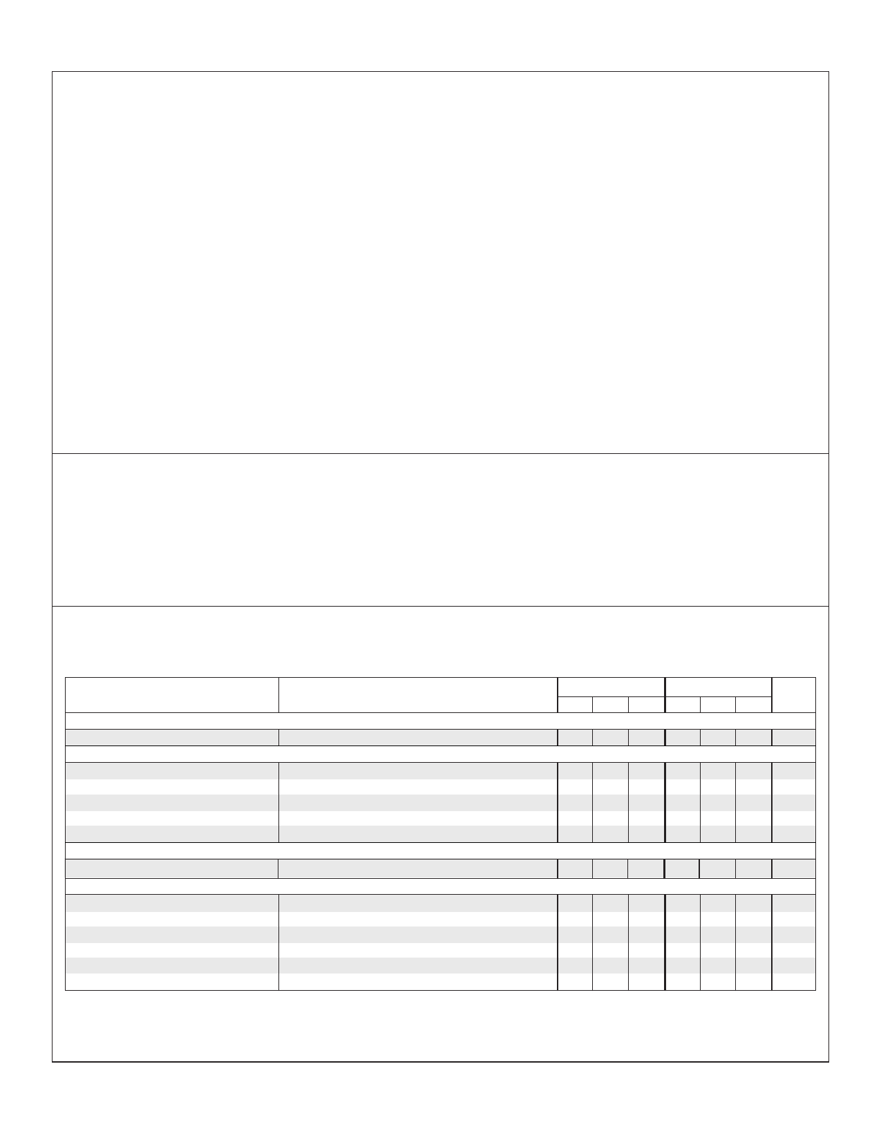
ELECTRICAL CHARACTERISTICS
(Unless
otherwise
specified,
these
specifications
apply
over
the
operating
ambient
temperatures
for
SG1548
with
-55 °C
≤
T
A
≤
125°C,
SG2548
with
-25°C ≤ TA ≤ 85°C, SG3548 with 0°C ≤ TA ≤ 70°C, and +VIN = 15V. Low duty cycle pulse testing techniques are used which maintains junction and case
temperatures equal to the ambient temperature.)
Parameter
Test Conditions
Supply Section
Supply Current
Reference Section (Note 4)
Output Voltage
Line Regulation
Load Regulation
Short Circuit Current
Fault Window Generator Section
Input Bias Current
DC Sense Inputs Section
Overvoltage Threshold
Undervoltage Threshold
Input Bias Current
Threshold Supply Rejection
+VIN = 40V
TJ = 25°C
Over Temperature
+V = 4.5V to 35V
IN
IL = 0 to 10mA
VREF = 0V
V = 1.5V to 2.45V
PIN 1
V = 0.95 x V
PIN 1
REF
VPIN 1 = 0.60 x VREF
VPIN 1 = 0.95 x VREF
VPIN 1 = 0.60 x VREF
VSENSE = 1.5V to 3.5V
+VIN = 4.5V to 35V
SG1548/2548
SG3548
Units
Min. Typ. Max. Min. Typ. Max.
4.8 10
4.8 10 mA
2.475 2.500 2.525 2.475 2.500 2.525 V
2.450
2.550 2.450
2.550 V
15
1 5 mV
3 10
3 10 mV
10 25 50 10 25 50 mA
-0.4 -2.0
-0.4 -2.0 µA
2.547 2.625 2.704 2.547 2.625 2.704 V
3.396 3.500 3.606 3.396 3.500 3.606 V
2.304 2.375 2.447 2.304 2.375 2.447 V
1.455 1.500 1.545 1.455 1.500 1.545 V
±0.6 ±2.0
±0.6 ±2.0 µA
60 100
60 100
dB
Note 4. I = 0mA
L
11/91 Rev 1.3 9/02
Copyright © 1997
LINFINITY Microelectronics Inc.
11861 Western Avenue ∞ Garden Grove, CA 92841
2
(714) 898-8121 ∞ FAX: (714) 893-2570
Share Link: 