USB1T1105A Просмотр технического описания (PDF) - Fairchild Semiconductor
Номер в каталоге
Компоненты Описание
производитель
USB1T1105A Datasheet PDF : 12 Pages
| |||
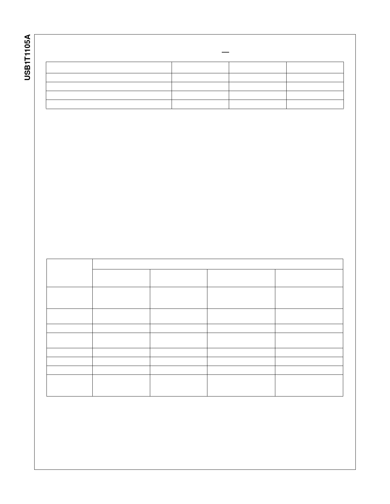
Note 4: SE0 = Single Ended Zero
TABLE 4. Receiver Function (OE = H)
D, D
Differential Logic 1
Differential Logic 0
SE0
Sharing Mode
RCV
Vp
Vm
H
H
L
L
L
H
X
L
L
L
H
H
X = Don’t Care
Power Supply Configurations and Options
The three modes of power supply operation are:
• Normal Mode: Regulated Output and Regulator Bypass
1. Regulated Output: VCCIO is connected and VCC (5.0) is
connected to 5V (4.0V to 5.5V) and the internal voltage
regulator then produces 3.3V for the USB connections.
2. Internal Regulator Bypass Mode: VCCIO is connected and
both VCC(5.5) and VREG(3.3) are connected to a 3.3V
source (3.0V to 3.6V).
In both cases for normal mode the VCCIO is an independent
voltage source (1.65V to 3.6V) that is a function of the exter-
nal circuit configuration.
• Sharing Mode: VCCIO is only supply connected. VCC and
VREG are not connected. In this mode the D and D pins are
3-STATE and the USB1T1105A allows external signals up to
3.6V to share the D and D bus lines. Internally the circuitry
limits leakage from D and D pins (maximum 10 PA) and
VCCIO such that device is in low power (suspended) state.
Terminals Vbusmon and RCV are forced LOW as an indica-
tion of this mode with Vbusmon being ignored during this
state.
• Disable Mode: VCCIO is not connected. VCC is connected, or
VCC and VREG are connected. 0V to 3.3V in this mode D and
D are 3-STATE and VPU is HIGH Impedance (switch is
turned off). The USB1T1105A allows external signals up to
3.6V to share the D and D bus lines. Internally the circuitry
limits leakage from D and D terminals (maximum 10PA).
A summary of the Supply Configurations is described in Table 5.
Pins
VCC
(5V)
TABLE 5. Power Supply Configuration Options
Power Supply Mode Configuration
Sharing
3.6V
Disable
Connected
to 5V Source
Normal
(Regulated Output)
Connected to 5V Source
VREG (3.3V)
VCCIO
VPU (3.3V)
Pulled LOW
Regulator OFF
1.65V to 3.6V Source
3-STATE (Off)
D, D
Vp, Vm
RCV
OE, SUSPND,
Config, Vpo/Vo,
Vmo/FSEO, MODE
3-STATE
H
L
Hi-Z
3.3V, 300 PA
Regulated Output
Not Connected
3-STATE (Off)
3-STATE
Invalid
Invalid
Hi-Z
3.3V, 300 PA
Regulated Output
1.65V to 3.6V Source
3.3V Available if
Config = HIGH
Function of Mode Set Up
Function of Mode Set Up
Function of Mode Set Up
Function of Mode Set Up
Normal
(Regulator Bypass)
Connected to VREG (3.3V)
[max drop of 0.3V]
(2.7V to 3.6V)
Connected
to 3.3V Source
1.65V to 3.6V Source
3.3V Available if
Config = HIGH
Function of Mode Set Up
Function of Mode Set Up
Function of Mode Set Up
Note 5: Hi-Z or forced LOW.
www.fairchildsemi.com
4
Share Link: 