USB1T1105A Просмотр технического описания (PDF) - Fairchild Semiconductor
Номер в каталоге
Компоненты Описание
производитель
USB1T1105A Datasheet PDF : 12 Pages
| |||
Terminal Terminal
Number Name
15
VPU (3.3V)
16
Exposed
Diepad
Config
GND
I/O
I
GND
Terminal Description
Pull-up Supply Voltage (3.3V r 10%):
Connect an external 1.5k: resistor on D (FS data rate);
Pin function is controlled by Config input pin:
Config = LOW VPU (3.3V) is floating (High Impedance) for zero pull-up current.
Config = HIGH VPU (3.3V) = 3.3V; internally connected to VREG (3.3V).
USB connect or disconnect software control input.
Configures 3.3V to external 1.5k: resistor on D when HIGH.
GND supply down bonded to exposed diepad to be connected to the PCB GND.
Functional Description
The USB1T1105A transceiver is designed to convert CMOS
data into USB differential bus signal levels and to convert USB
differential bus signal to CMOS data.
To minimize EMI and noise the outputs are edge rate controlled
with the rise and fall times controlled and defined for full speed
data rates. The rise, fall times are balanced between the differ-
ential pins to minimize skew.
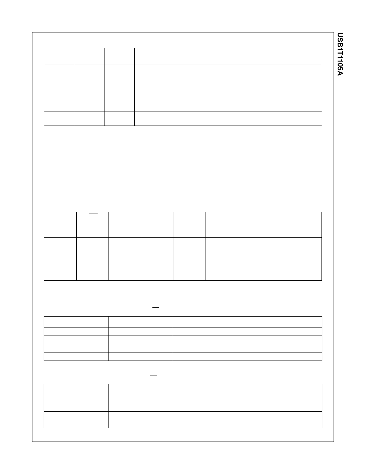
Table 1 describes the specific pin functionality selection. Table
2, Table 3, and Table 4 describe the specific Truth Tables for
Driver and Receiver operating functions.
The USB1T1105A also has the capability of various power sup-
ply configurations to support mixed voltage supply applications
(see Table 5) and Power Supply Configurations and Options for
detailed descriptions.
Functional Tables
TABLE 1. Function Select
SUSPND
OE
L
L
L
H
H
L
H
H
D, D
Driving &
Receiving
Receiving
(Note 1)
Driving
3-STATE
(Note 1)
RCV
Active
Active
Inactive
(Note 2)
Inactive
(Note 2)
Vp/Vm
Active
Active
Function
Normal Driving
(Differential Receiver Active)
Receiving
Active
Active
Driving during Suspend
(Differential Receiver Inactive)
Low Power State
Note 1: Signal levels is function of connection and/or pull-up/pull-down resistors.
Note 2: For SUSPND = HIGH mode the differential receiver is inactive and the output RCV output is forced LOW. The out-of-suspend signaling (K) is detected via the single-
ended receiver outputs of the Vp and Vm pins.
TABLE 2. Driver Function (OE = L) using Differential Input Interface Mode Pin = H
Vmo
L
L
H
H
Vpo
L
H
L
H
Data
SE0 (Note 3)
Differential Logic 1
Differential Logic 0
Illegal State
Note 3: SE0 = Single Ended Zero
TABLE 3. Driver Function (OE = L) using Single-ended Input Interface Mode Pin = L
FSE0
Vo
L
L
L
H
H
L
H
H
Data
Differential Logic 0
Differential Logic 1
SE0 (Note 4)
SE0 (Note 4)
3
www.fairchildsemi.com
Share Link: 