USB1T1102 Просмотр технического описания (PDF) - Fairchild Semiconductor
Номер в каталоге
Компоненты Описание
производитель
USB1T1102 Datasheet PDF : 14 Pages
| |||
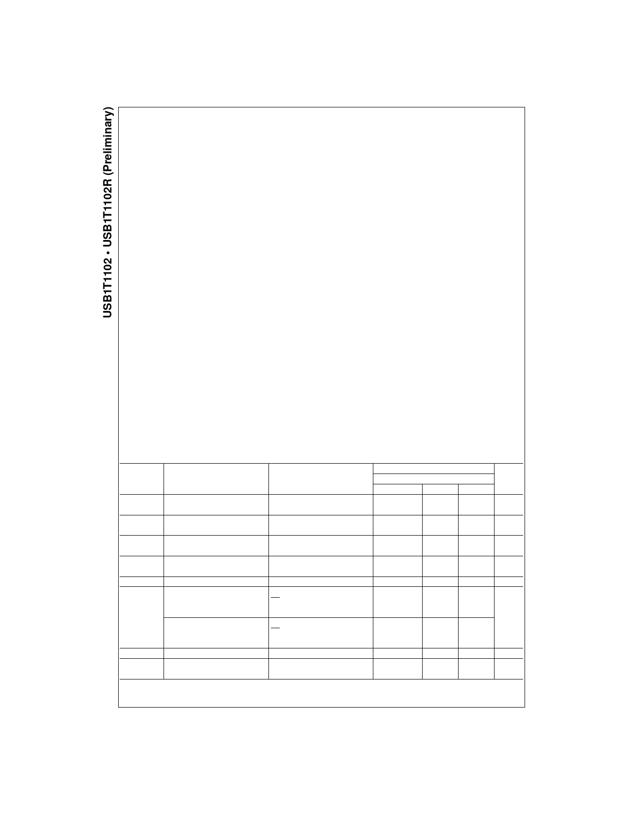
Absolute Maximum Ratings(Note 4)
Supply Voltage (VCC)(5V)
I/O Supply Voltage (VCCIO)
Latch-up Current (ILU)
VI = −1.8V to +5.4V
DC Input Current (IIK)
VI < 0
DC Input Voltage (VI)
(Note 5)
DC Output Diode Current (IOK)
VO > VCC or VO < 0
DC Output Voltage (VO)
(Note 5)
Output Source or Sink Current (IO)
VO = 0 to VCC
Current for D+, D− Pins
−0.5V to +6.0V
−0.5V to +4.6V
150 mA
−50 mA
−0.5V to VCCIO +5.5V
±50 mA
−0.5V to VCCIO + 0.5V
±50 mA
Current for RCV, Vm/Vp
DC VCC or GND Current
(ICC, IGND)
ESD Immunity Voltage (VESD);
Contact HBM
±15 mA
±100 mA
Pins D+, D−, VCC (5.5V) and GND
All Other Pins
15kV
6.5kV
Storage Temperature (TSTO)
Power Dissipation (PTOT)
ICC (5V)
ICCIO
−40°C to + 125°C
48 mW
9 mW
Recommended Operating
Conditions
DC Supply Voltage VCC (5V)
I/O DC Voltage VCCIO
DC Input Voltage Range (VI)
DC Input Range for AI/O (VAI/O)
Pins D+ and D−
Operating Ambient Temperature
(TAMB)
4.0V to 5.5V
1.65V to 3.6V
0V to VCCIO +5.5V
0V to VCC
0V to 3.6V
−40°C to +85°C
Note 4: The Absolute Maximum Ratings are those values beyond which
the safety of the device cannot be guaranteed. The device should not be
operated at these limits. The parametric values defined in the Electrical
Characteristic tables are not guaranteed at the absolute maximum rating.
The “Recommended Operating Conditions” table will define the conditions
for actual device operation.
Note 5: IO Absolute Maximum Rating must be observed.
DC Electrical Characteristics (Supply Pins)
Over recommended range of supply voltage and operating free air temperature (unless otherwise noted).
VCC (5V) = 4.0V to 5.5V or VREG (3.3V) = 3.0V to 3.6V, VCCIO = 1.65V to 3.6V
Limits
Symbol
Parameter
Conditions
−40°C to +85°C
Min
Typ
VREG (3.3V)
ICC
ICCIO
Regulated Supply Output
Operating Supply Current (VCC5.0)
I/O Operating Supply Current
Internal Regulator Option;
ILOAD ≤ 300 µA
Transmitting and Receiving at
12 Mbits/s; CLOAD = 50 pF (D+, D−)
Transmitting and Receiving at
12 Mbits/s
3.0
(Note 6)(Note 7)
3.3
4.0
(Note 8)
1.0
(Note 8)
ICC (IDLE)
ICCIO (STATIC)
ICC(SUSPND)
Supply Current during
FS IDLE and SE0 (VCC5.0)
I/O Static Supply Current
Suspend Supply Current
USB1T1102
IDLE: VD+ ≥ 2.7V, VD− ≤ 0.3V;
SE0: VD+ ≤ 0.3V, VD− ≤ 0.3V
IDLE, SUSPND or SE0
SUSPND = HIGH
OE = HIGH
Suspend Supply Current
Vm = Vp = OPEN
SUSPND = HIGH
USB1T1102R
OE = HIGH
ICCIO(SHARING) I/O Sharing Mode Supply Current
ID+ (SHARING) Sharing Mode Load Current on
D+/D− Pins
Vp = Vm = OPEN
VCC (5V) Not Connected
VCC (5V) Not Connected
Config = LOW; VD± = 3.6V
Max
3.6
8.0
2.0
300
(Note 9)
20.0
25.0
(Note 9)
40.0
(Note 10)
20.0
10.0
Units
V
mA
mA
µA
µA
µA
µA
µA
www.fairchildsemi.com
6
Share Link: 