US3011CW Просмотр технического описания (PDF) - Unisem
Номер в каталоге
Компоненты Описание
производитель
US3011CW Datasheet PDF : 11 Pages
| |||
US3011
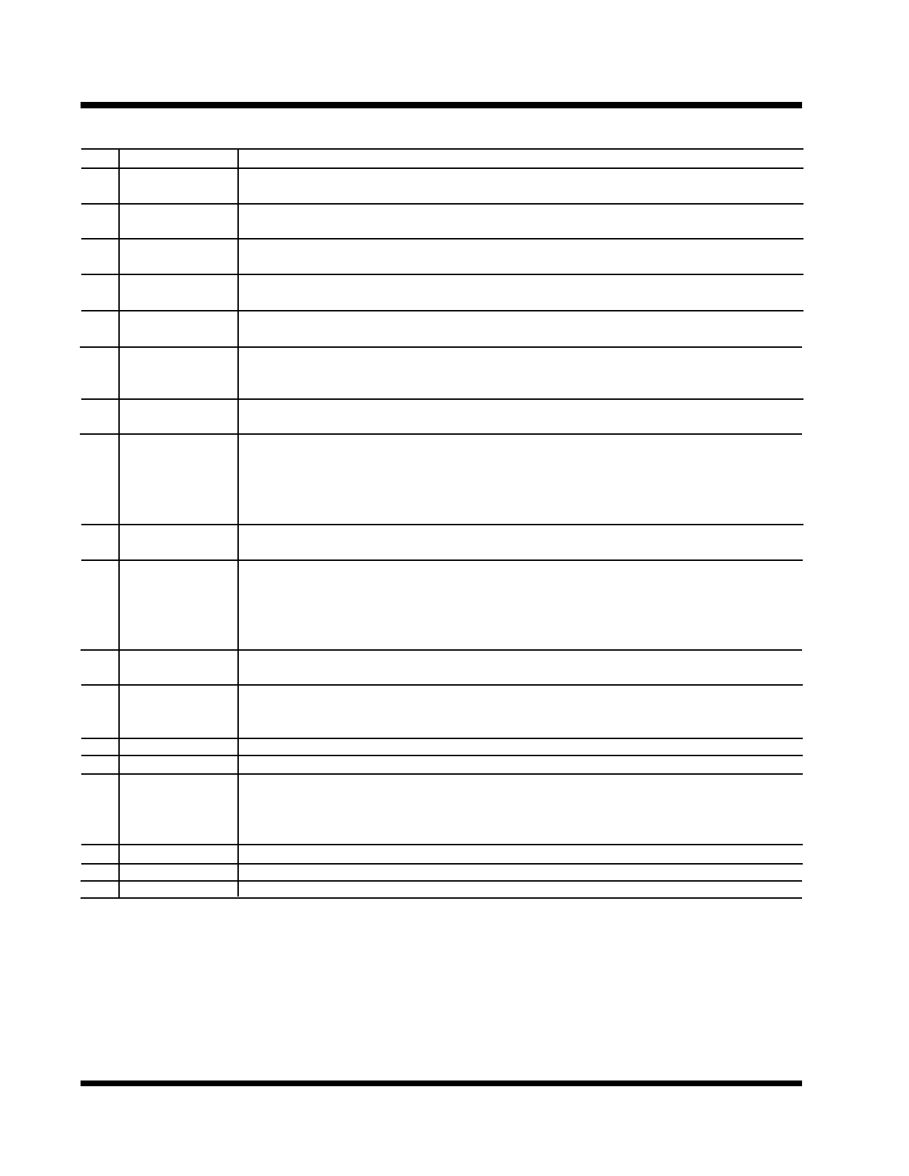
PIN DESCRIPTIONS
PIN# PIN SYMBOL
4 D0
5 D1
6 D2
7 D3
8 D4
Pin Description
LSB input to the DAC that programs the output voltage. This pin can be pulled up exter-
nally by a 10k resistor to either 3.3V or 5V supply.
Input to the DAC that programs the output voltage.This pin can be pulled up externally by
a 10kΩ resistor to either 3.3V or 5V supply.
Input to the DAC that programs the output voltage.This pin can be pulled up externally by
a 10k resistor to either 3.3V or 5V supply.
MSB input to the DAC that programs the output voltage.This pin can be pulled up exter-
nally by a 10k resistor to either 3.3V or 5V supply.
This pin selects a range of output voltages for the DAC.
12 PGd
10 Vfb
2 CS+
13 CS-
3 SS
20 Ct
16 Gnd
17 LDrv
14 HDrv
18 V12
9 V5
19 OVP
15,11 NC
This pin is an open collector output that switches LO when the output of the converter is
not within ±10% (typ) of the nominal output voltage.When PWRGD pin switches LO the
sat voltage is less than 0.4V at 3mA.
This pin is connected directly to the output of the Core supply to provide feedback to the
Error comparator.
This pin is connected to the Drain of the power MOSFET of the Core supply and it
provides the positive sensing for the internal current sensing circuitry. An external resis-
tor programs the C.S threshold depending on the Rds of the power MOSFET. An external
capacitor is placed in parallel with the programming resistor to provide high frequency
noise filtering.
This pin is connected to the Source of the power MOSFET for the Core supply and it
provides the negative sensing for the internal current sensing circuitry.
This pin provides the soft start for the switching regulator. An internal current source
charges an external capacitor that is conected from this pin to the GND which ramps up
the outputs of the switching regulator, preventing the outputs from overshooting as wellas
limiting the input current. The second function of the Soft Start cap is to provide long off
time for the synchronous MOSFET or the Catch diode (HICCUP) during current limiting.
This pin programs the oscillator frequency in the range of 50 kHZ to 500kHZ with an
external capacitor connected from this pin to the GND.
This pin serves as the ground pin and must be conected directly to the ground plane. A
high frequency capacitor (0.1 to 1 uF) must be connected from V5 and V12 pins to this
pin for noise free operation.
Output driver for the synchronous power MOSFET.
Output driver for the high side power MOSFET.
This pin is connected to the 12 V supply and serves as the power Vcc pin for the output
drivers.A high frequency capacitor (0.1 to 1 uF) must be connected directly from this pin
to GND pin in order to supply the peak current to the power MOSFET during the transi-
tions.
5V supply voltage.
Over voltage comparator output.
No connect
4-4
Rev. 1.3
12/8/00
Share Link: 