UPD75236GJ Просмотр технического описания (PDF) - NEC => Renesas Technology
Номер в каталоге
Компоненты Описание
производитель
UPD75236GJ Datasheet PDF : 190 Pages
| |||
µPD75236
3.3 DATA MEMORY
The data memory consists of a static RAM and peripheral hardware.
The static RAM incorporates 512 words × 4 bits of memory banks 0 and 2, 160 words × 4 bits of memory
bank 1 and 96 words × 4 bits of memory bank 1 which also serves as a display data memory. It is used to store
process data and to serve as a stack memory for interrupt execution.
General registers, display data memory and various registers of peripheral hardware are mapped at particu-
lar addresses of the data memory and such data is manipulated by the general register and memory manipula-
tion instructions. (Refer to Fig. 2-1 Data Memory Configuration and Addressing Range in Each Addressing
Mode.)
All addresses (000H to 2FFH) of memory banks 0, 1 and 2 can be used as a stack area.
Although the data memory consists of one address and 4 bits, it can be manipulated in 8-bit units by the 8-
bit memory mainipulation instruction or in bit units by the bit manipulation instruction. Specify an even
address by the 8-bit manipulation instruction.
The display data memory area (1A0H to 1FFH) is made up as shown in Fig. 3-4.
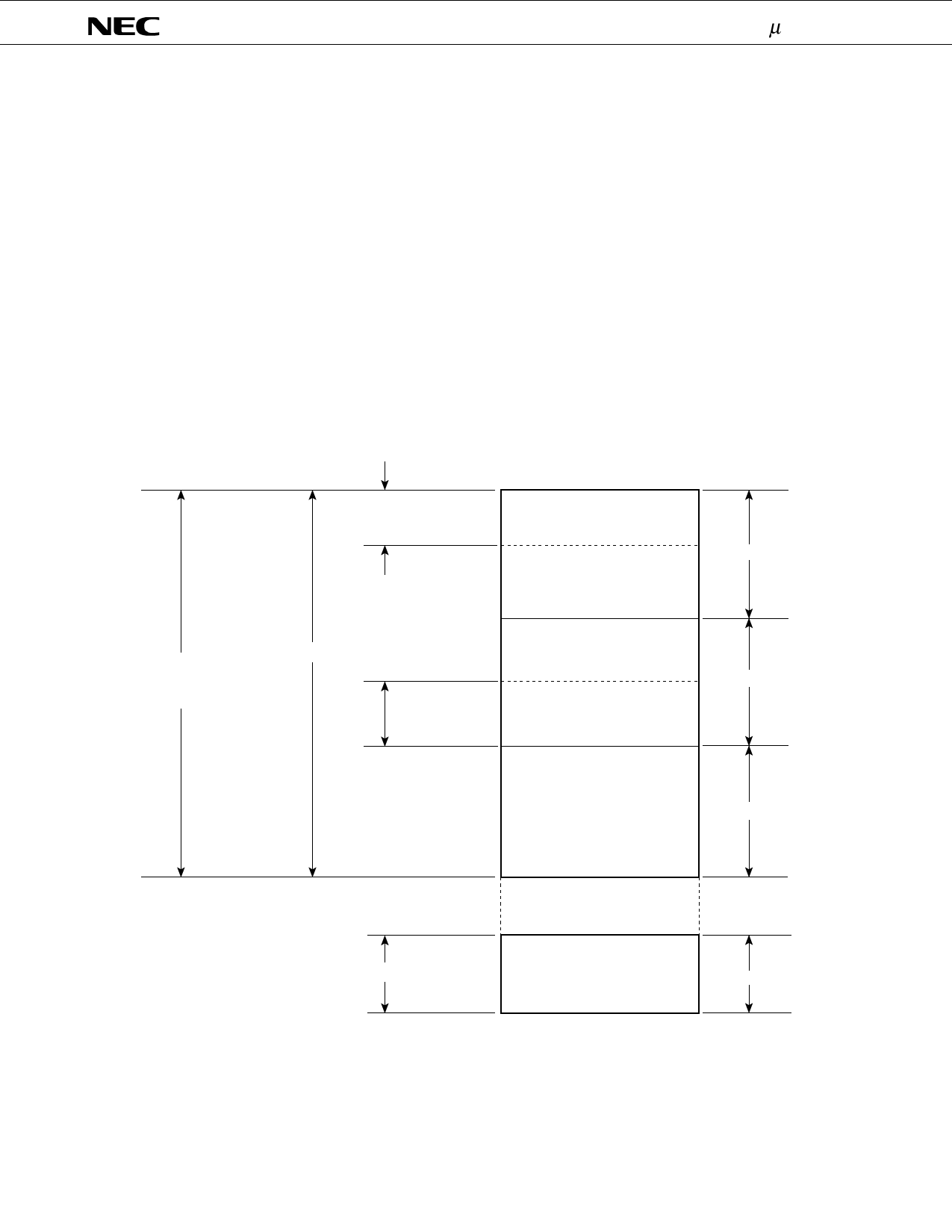
Fig. 3-3 Data Memory Map
Data Area
Static RAM
(768 × 4)
General
Register
Area
Stack Area
Display
Data
Memory,
etc.
000H
01FH
020H
0FFH
100H
19FH
1A0H
1FFH
200H
Data Memory
(32 × 4)
256 × 4
256 × 4
(96 × 4)
Memory Bank
0
1
256 × 4
2
2FFH
Not Incorporated
F80H
Peripheral Hardware Area
128 × 4
15
FFFH
30
Share Link: 