UPD75236GJ Просмотр технического описания (PDF) - NEC => Renesas Technology
Номер в каталоге
Компоненты Описание
производитель
UPD75236GJ Datasheet PDF : 190 Pages
| |||

µPD75236
2.2 GENERAL REGISTER BANK CONFIGURATION
The µPD75236 incorporates four register banks, each bank consisting of eight general registers, X, A, B, C,
D, E, H and L. This general register area is mapped at addresses 00H to 1FH of the memory bank 0 of the data
memory (refer to Fig. 2-2 General Register Configuration (4-Bit Processing)). A register bank enable flag (RBE)
and a register bank select register (RBS) are incorporated to specify the above general register banks. RBS is a
register to select a register bank and RBE is a flag to determine whether the register bank selected by RBS
should be validated or not. The register bank (RB) which is validated for instruction execution is given as
RB = RBE• RBS.
As described above, with the µPD75236 having four register banks, programs can be created very efficiently
by using different register banks for normal processing and interrupt service as described in Table 2-2. (RBE is
automatically saved and set for interrupt service and automatically reset upon termination of the interrupt
service.)
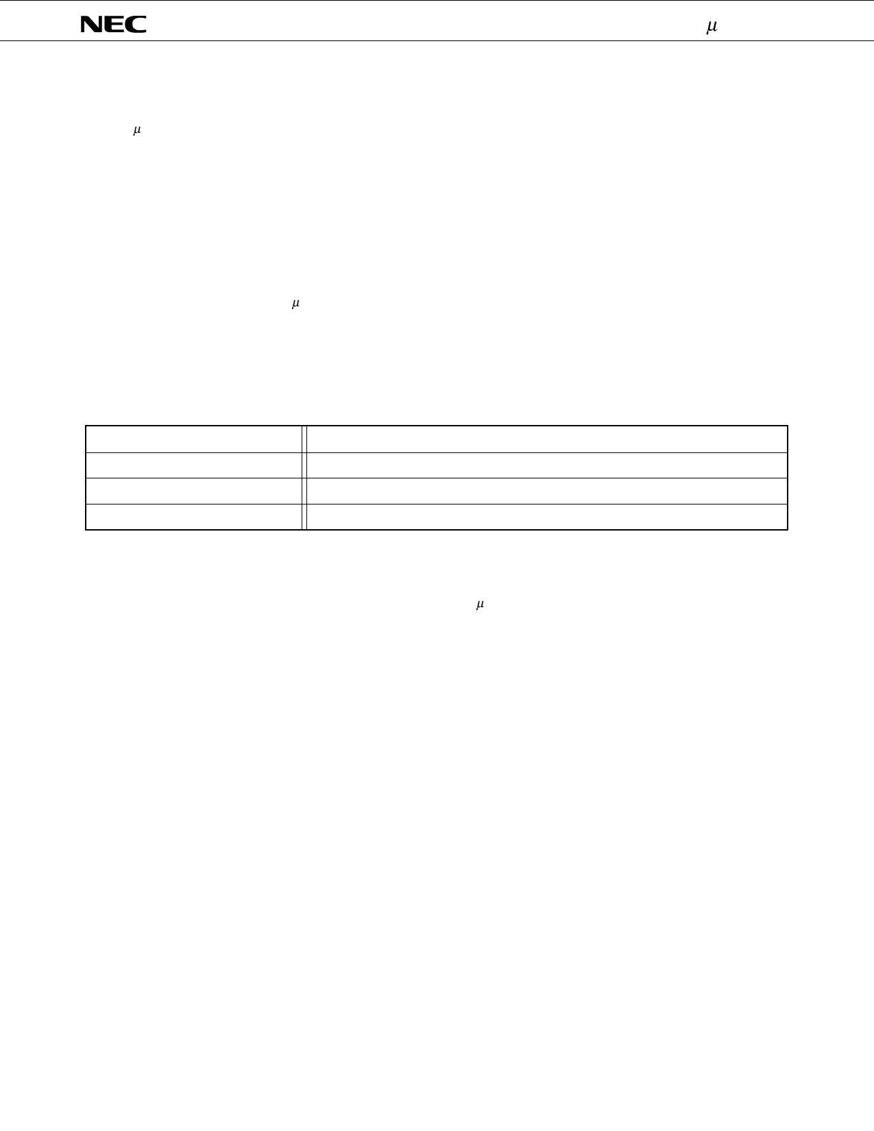
Table 2-2 Recommended Use of Register Banks in Normal and Interrupt Routines
Normal processing
Single interrupt service
Double interrupt service
Triple or more interrupt service
Use register banks 2 and 3 with RBE = 1.
Use register bank 0 with RBE = 0.
Use register bank 1 with RBE = 1. (It is necessary to save/reset RBS.)
Save/reset registers by PUSH and POP.
Not only in 4-bit units, a register pair of XA, HL, DE or BC can transfer, compare, operate, increment or
decrement data in 8-bit units. In this case, register pairs with the reversed bit 0 of the register bank specified by
RBE• RBS can be specified as XA’, HL’, DE’ and BC’. Thus, the µPD75236 has eight 8-bit registers (refer to Fig. 2-
3 General Register Configuration (8-Bit Processing)).
19