UPD6464A Просмотр технического описания (PDF) - NEC => Renesas Technology
Номер в каталоге
Компоненты Описание
производитель
UPD6464A
UPD6464A Datasheet PDF : 52 Pages
| |||

µPD6464A,6465
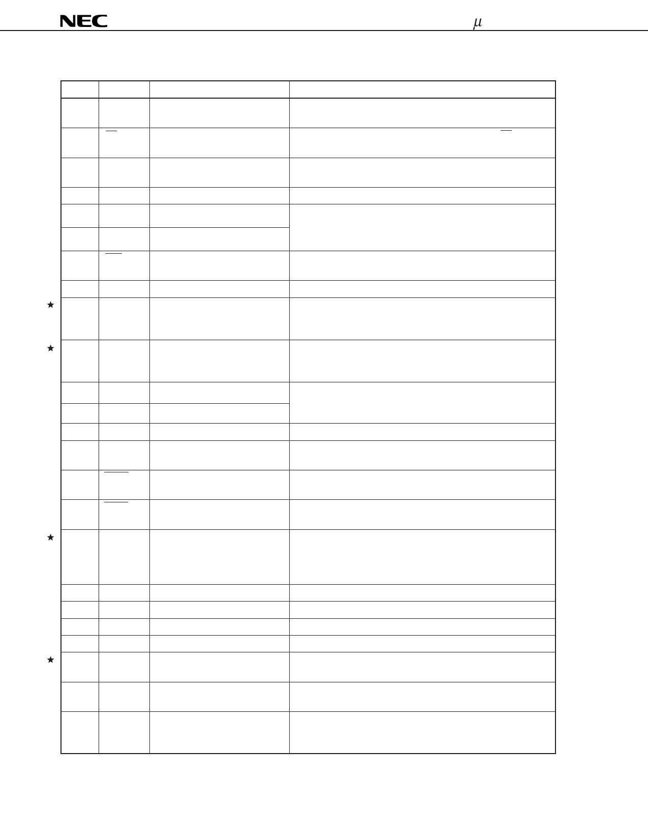
PIN FUNCTIONS
No.
Symbol
Pin Name
1
CLK
Clock input
2
CS
Chip select input
Function
Inputs clock for data read. Data input to the DATA pin is read at
the rising edge of the clock input to this pin.
Serial transfer can be acknowledged by making this CS pin low.
3
DATA
Serial data input
4
VDD
Power supply
5
OSCOUT
LC oscillation output
6
OSCIN
LC oscillation input
Inputs control data. Data is read in synchronization with the clock
input to the CLK pin.
Supplies power to the IC.
These are input and output pins of an oscillator that generates
dot clocks. Connect a coil and a capacitor to these pins for
oscillation.
7
PCL
Power-ON clear
Power-ON clear pin. Make this pin high on power application. It
initializes the internal circuitry of the IC.
8
GND
Ground
Ground pin of the IC.
9
FSCI
fSC signal input
In case of the ×4 multiplier, the color sub-carrier (fSC) is input to
this pin. In case of the 4fSC Crystal oscillation, connect this pin to
GND or VDD.
10 FSCO
Frequency error output
The frequency error signal of the ×4 multiplier is output to this
pin. In case of the 4fSC Crystal oscillation, this pin should be
open.
11 XOSO
12 XOSI
Quadruple oscillation output
Quadruple oscillation input
A quadruple oscillation LC for internal video signal generation is
connected to these pins. A crystal oscillator can also be
connected.
13
VC
Character signal output
Character signal output pin. Positive signal output.
14
VBLK
15 HSYO
Blanking signal output
Horizontal synchronization signal
output
This pin outputs a blanking signal that cuts the video signal. It
corresponds to the output of VC. Positive signal output.
Outputs a horizontal synchronization signal separated from a
composite synchronization signal.
16 VSYO
Vertical synchronization signal
output
Outputs a vertical synchronization signal separated from a
composite synchronization signal.
17 CSYIN
18 N. C.
Composite synchronization signal
input
A composite synchronization signal is input to this pin for
synchronization signal separation. In case of the external signal
mode, input the signal certainly. Input a positive synchronization
signal.
Non connection
Non connection. Leave this pin open.
19 TEST
Test pin
Test mode select pin. Connect this pin to GND.
20 NRE
21 VBSO
Noise reduction constant append Constant append pin for noise reduction.
Composite video signal output
Outputs a composite video signal mixing a character signal.
22 SECAM SECAM subcarrier input
SECAM sub-carrier signal mixing pin. In cases of any system
except for SECAM, this pin should be open.
23
VCNT
24 VBSI
Video signal output level adjust-
ment
Composite video signal input
Adjusts the output level of the composite video signal and
luminance signal.
Inputs a composite video signal. Inputs a signal with the leading
edge clamped, consisting of a negative synchronization signal
and a positive video signal.
4