UPD6461GS –ü—Ä–æ—Å–º–æ—Ç—Ä —Ç–µ—Ö–Ω–∏—á–µ—Å–∫–æ–≥–æ –æ–ø–∏—Å–∞–Ω–∏—è (PDF) - NEC => Renesas Technology
–ù–æ–º–µ—Ä –≤ –∫–∞—Ç–∞–ª–æ–≥–µ
–ö–æ–º–ø–æ–Ω–µ–Ω—Ç—ã –û–ø–∏—Å–∞–Ω–∏–µ
–ø—Ä–æ–∏–∑–≤–æ–¥–∏—Ç–µ–ª—å
UPD6461GS
NEC => Renesas Technology

UPD6461GS Datasheet PDF : 60 Pages
| |||
µPD6461, 6462
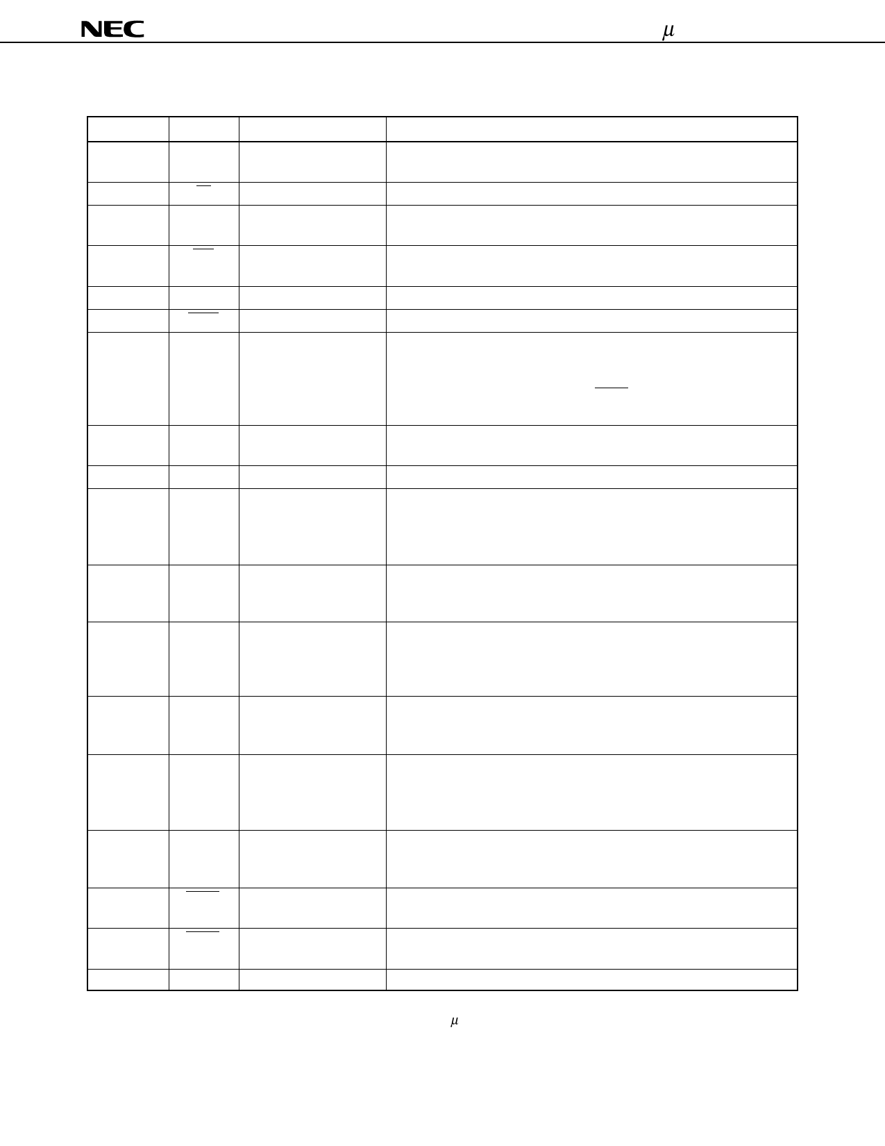
PIN FUNCTIONS
Pin No.Note 1 SymbolNote 2
FunctionNote 2
1
CLK
Clock input
2
3 (4)
CS
DATA
Chip select input
Serial data input
4 (5)
PCL
Power-on clear
5 (6)
6 (7)
7 (8)
8 (9)
VDD
CKOUT
OSCOUT
OSCIN
Power supply
Clock output
LC oscillator input/
output
OSCIN: External clock
input
9 (10)
TEST Test pin
10 (11)
11 (14)
GND
BLK1
Ground pin
Blanking signal output 1
12 (15)
13 (16)
VC1
Character signal output
1
BLK2
(RBLK)
Blanking signal output 2
(blanking R)
14 (17)
15 (18)
VC2
(GBLK)
VBLK
(BBLK)
Character signal output
2
(blanking G)
Blanking signal output
(blanking B)
16 (19)
17 (20)
18 (21)
19 (23)
VR
VG
VB
Vsync
20 (24)
Hsync
(3, 12, 13, 22) N.C.
Character signal output
Vertical synchronizing
signal input
Horizontal synchroniz-
ing signal input
No connection
Description
Input pin for the data read clock. The data input to the DATA pin is read at
rising edges of the clock.
Serial transfer is accepted when this pin is low.
Input pin for control data. Data is read in synchronization with the clock input
to the CLK pin.
Pin used for the power-on clear function. After power-on, set this pin from low
to high to initialize the IC.
Power supply pin
N-ch open-drain output pin used to check the oscillation frequency
Input and output pins for the oscillator for generating a dot clock. Connect
the oscillation coil and capacitors to these pins.
(When an external clock input is selected by specifying a mask option, input
an external clock (synchronized with Hsync) to the OSCIN pin. Leave the
OSCOUT pin open.)
Pin used for testing the IC. Usually, connect this pin to ground. The IC cannot
enter test mode while this pin is connected to ground.
Connect this pin to the system ground.
Pin used to output the blanking signal for the video signal output from the VC1
pin. The blanking signal is high active.
(When RGB compatible blanking has been selected by specifying a mask
option, this pin outputs the logical OR of RBLK, GBLK, and BBLK.)
Pin used to output a high-active character signal.
(When RGB compatible blanking has been selected by specifying a mask
option, this pin outputs the logical OR of VR, VG, and VB.)
Pin used to output the blanking signal for the video signal output from the VC2
pin. The blanking signal is high active.
(This pin outputs the blanking signal for the video signal output from the VR
pin. The blanking signal is high active.)
Pin used to output a high-active character signal.
(This pin outputs the blanking signal for the video signal output from the VG
pin. The blanking signal is high active.)
Pin used to output the blanking signal for the video signals output from the
VR, VG, and VB pins. The blanking signal is high active.
(This pin outputs the blanking signal for the video signal output from the VB
pin. The blanking signal is high active.)
Pins used to output high-active character signals.
Input a low-active vertical synchronizing signal to this pin.
Input a low-active horizontal synchronizing signal to this pin.
Vacant pin
Notes 1. Pin numbers indicated in ( ) are that of the µPD6461GT-xxx.
2. Signals in ( ) are set by a mask option (RGB + RGB compatible blanking).
6
Share Link: